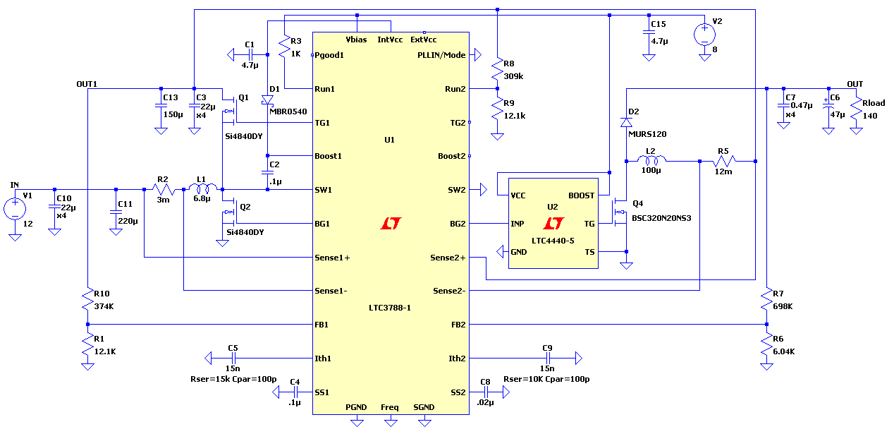
LTC3788 Generates High Voltages Using a Two-Stage Boost Converter
LTC3788 Generates High Voltages Using a Two-Stage Boost Converter
Sep 17 2014
Generating high voltages from low level sources is not an easy task. Engineers are facing the following problems when they try to implement single stage boost at high step-up ratios.
- Limitation of maximum duty cycle in boost controllers
- Sharp decrease in efficiency at long duty cycles
- High peak currents and EMI challenges when moving converter from continuous-conduction-mode (CCM) to discontinuous-conduction-mode (DCM) to shorten the duty cycle
One way to solve this problem is the use of a two-stage boost converter. The first stage produces an intermediate voltage rail, which is then boosted to the desirable high voltage level by the second stage. The LTC3788 is a very good candidate to implement this topology on a single controller. LTC3788 is a high performance 2-phase dual synchronous boost converter controller that drives all N-channel power MOSFETs. The first stage can take advantage of synchronous rectification, which increases efficiency, reduces power losses and eases thermal requirements. Maximum ABS rating switching pins of this controller is 70V and this is the limit of using synchronous rectification on the second stage. However, it can be easily rewired to nonsynchronous, if higher voltages levels than 70V are needed.

LTC3788-1 & LTC4440-5 - Two-Stage High Voltage Boost Converter
The schematic shown above and the LTspice simulation of the LTC3788-1 controller for two-stage boost converter illustrate a solution for output voltage greater than 70V. The input voltage through a sense resistor and an inductor is boosted by the synchronous first stage to the intermediate level, which then becomes the input voltage for the non- synchronous second stage. The input voltage range of this circuit is 3V to 36V, nominal 12V, and the output is 140V at 1A. However, the output current will be reduced at input voltages below 10V.
The schematic also reflects two limitations of this approach. Maximum ABS rating of SENSE pins is 40V and output of the first stage should not exceed this level, because it is an input for second stage. Also INTVcc and the gate voltage of the switching FETs is 5V. This is not enough for high voltage applications where standard FETs are used with gate voltages 7V to 12V. Therefore, an LDO is used to bias the LTC4440 High Voltage High Side Gate Driver and LTC3788. Alternately, a buck converter can be employed to increase efficiency.
About the Authors
Victor Khasiev was a senior applications engineer at ADI with extensive experience in power electronics both in ac-to-dc and dc-to-dc conversion. He holds two patents and has written multiple articles. These articles are r...
Gabino Alonso is currently the director of strategic marketing for the Power by Linear™ Group. Prior to joining ADI, Gabino held various positions in marketing, engineering, operations, and education at Linear Technology, ...
Related to this Article
Products
PRODUCTION
2-Phase, Dual Output Synchronous Boost Controller
PRODUCTION
High Speed, High Voltage, High Side Gate Driver
PRODUCTION
2-Phase, Dual Output Synchronous Boost Controller


