Low Noise Power Supplies Come in Many Flavors: Part 3 - Buck Converters
Low Noise Power Supplies Come in Many Flavors: Part 3 - Buck Converters
Mar 23 2017
Read other articles in this series.
In Part 1 of the series, we looked at linear regulators for lowest output noise performance. In Part 2, charge pump solutions with integrated post linear regulators we highlighted. In these previous examples, circuit efficiency was a lower priority. But what if low output voltage noise and high efficiency are both desired? Can a single chip solution suffice to provide both?
Low Noise Step-Down Switching Regulators
Switching regulator output noise depends on many factors such as peak inductor current, load current, switching regulator topology, circuit control loop techniques, size and characteristics of the output capacitor, circuit component values and layout. Analog Devices offers many devices that provide peak-to-peak noise levels less than 10mV over the entire load current and input supply voltage range.
Efficiency
With switch mode power supplies, high efficiency is difficult to obtain when the converter is lightly loaded because the control circuitry power dissipation and switching power losses become a much larger percentage of the power budget than they are at higher loads. Analog Devices' patented automatic Burst Mode technology allows a switch mode power supply to provide high efficiency even when lightly loaded, by turning off non-essential circuitry when the output is in regulation, but keeping a comparator actively monitoring the output so the control circuitry can quickly be turned on again when the output begins to droop. Then as the load current increases, the converter will automatically transition between Burst Mode to the lower noise PWM mode of operation. Conversely the converter will automatically transition from PWM operation to Burst Mode operation when the load decreases. Entry to and exit from the Burst Mode region depends on the input voltage, the output voltage and the inductor value but is typically less than 100mA. An application circuit using the LTC3103, which has the option for automatic Burst Mode operation, is shown below in Figure 1a. The efficiency versus output current for the LTC3103 is shown in Figure 1b. At a 5V input and a 2.2V, 100µA load current, the efficiency is an impressive 80.3% when Burst Mode is employed.
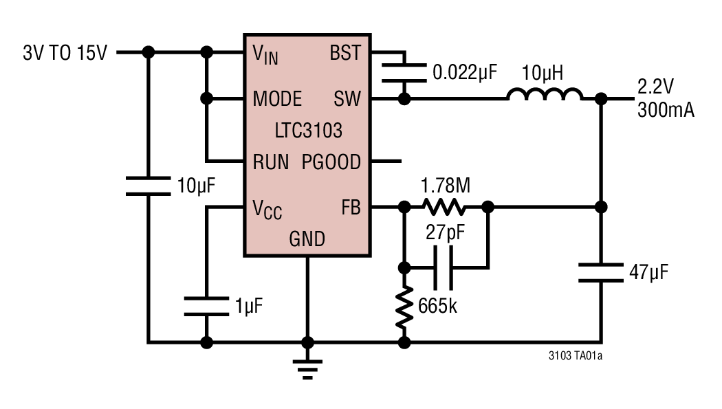
Figure 1a. LTC3103 Typical Operating Circuit.
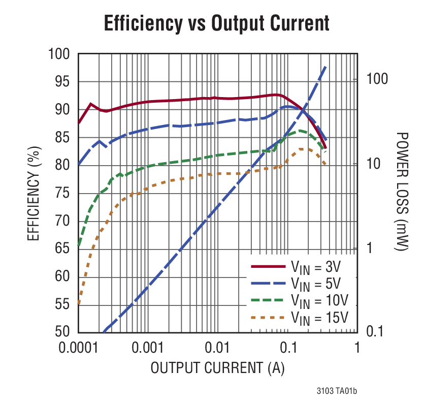
Figure 1b. LTC3103 Has High Efficiency Even with Light Loads.
Many parts on the market make claims about their best-in-class ultralow quiescent current and high efficiency. Several competing devices list lower quiescent current than the LTC3103's 1.8µA Burst Mode current, but their efficiency at light load is much worse. You are encouraged to compare our efficiency plot in Burst Mode to these devices. You will notice two things: our graph plots include efficiency numbers for sub-1mA load currents, and for efficiencies their plots do show our light load Burst Mode efficiencies are typically 25% to 45% higher for the same load currents.
Output Noise
When the load current is above the Burst Mode threshold and the converter transitions to PWM operation the output voltage noise is quite low, dependent only on inductor current ripple and output capacitor size. As the load current is decreased and the converter transitions to Burst Mode operation the control circuits are turned on and off intermittently to save power. Although the average output voltage is regulated accurately in this mode the output voltage hysteresis between the control circuit turn on and turn off points causes higher output voltage ripple resulting in increased subharmonic noise. A comparison of PWM (Figure 2a) and Burst Mode (Figure 2b) ripple for the same load current is shown in the example below.
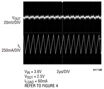
Figure 2a. Constant Frequency Switching Output Noise.
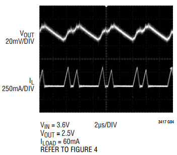
Figure 2b. Burst Mode Switching Output Noise.
A device like the LTC3103 gives high efficiency, but is its noise performance adequate? In many cases, the answer is yes. Analog Devices has improved Burst Mode performance over the years, resulting in even lower output voltage noise performance for more recently announced products. A graph of the LTC3103 output noise in Burst Mode is shown below. In this figure, the peak output noise ranges from about 10mV to 12mV.
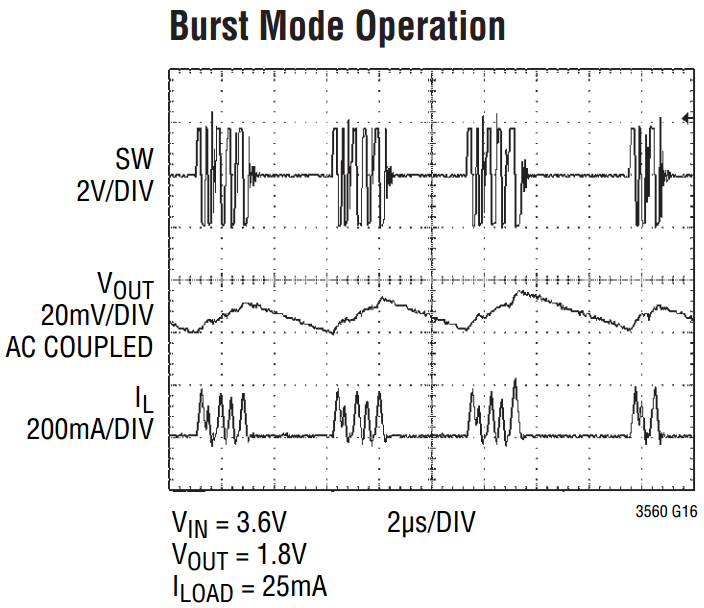
Figure 3. LTC3103 Burst Mode Output Noise.
Light load efficiency is the true upside of Burst Mode but if the noise performance in Burst Mode is an issue the customer has a couple of options. First, because the MODE pin controls the operating mode, the device can be momentarily switched into force continuous mode to minimize noise. This is ideal in applications like low power transmitters where the low noise mode is only needed when transmitting data or when a sensitive measurement is being taken. Forced continuous mode reduces the output noise, but at the expense of efficiency. If the degradation in efficiency is only for a short time, the overall system efficiency will only slightly be affected. Remember that even if enabled and the load current is high enough Burst mode automatically transitions to the lowest noise, constant frequency switch-on-every-cycle PWM mode. The figure below shows a 12V input converted to 3.3V@300mA and the peak output noise is only 5mV. The graphs Y and X scale axes are 10mV/div and 500ns/div respectively. As the input-to-output voltage differential is reduced, the output noise will also improve. Changing the input voltage to 5V reduces the output noise to 2mV peak-to-peak.
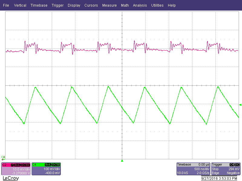
Figure 4. LTC3103: 12V to 3.3V@300mA.
A second option is to use the LTC3104 which is simply the LTC3103 with an integrated 10mA low dropout linear regulator. The linear regulator has a separate input supply pin and a 150mV typical dropout voltage.
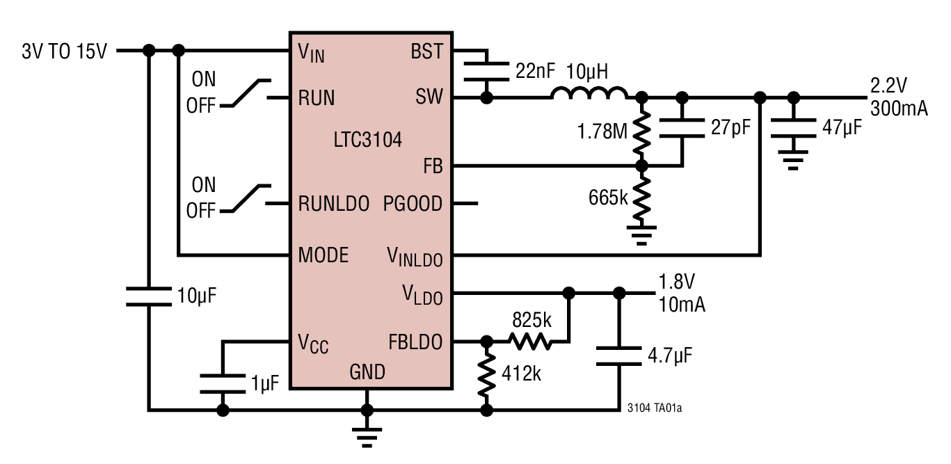
Figure 5. LTC3104 Adds a 10mA Low Noise Linear Regulator.
The figure below shows the LTC3104 with a 12V input, a 4V buck output and a 3.3V post-regulator LDO which reduces the 4V output to 3.3V@10mA. The Y and X scale axes again are 10mV/div and 500ns/div respectively. Note the peak-to-peak ripple on the LDO output (the middle trace) is now in the ±1mV range.
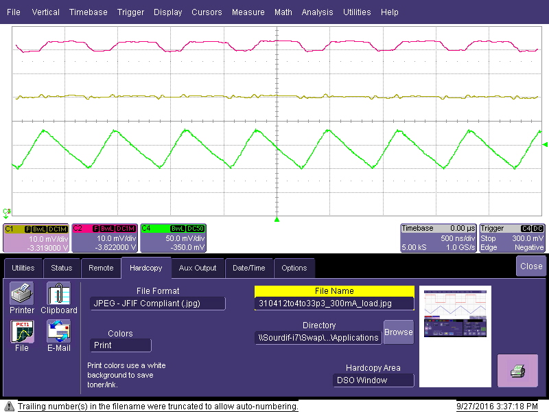
Figure 6. LTC3104 with Low Noise 10mA LDO Output.
A final option is to add a discrete filter or a ferrite bead at the output to reduce noise. However the specifics of how to select the right filtering components and values are very application specific and beyond the scope of this discussion.
In Summary
There are many power supply options for low noise, high efficiency systems. Sometimes the noise needs to be "low enough" as a tradeoff to improved light load efficiency, and at other times best noise performance is required for any load current. For any of these applications Analog Devices' extensive power supply offerings simplify the process of selecting your low noise solution. From best-in-class low noise linear regulators to single chip solution charge pumps with integrated LDOs and low noise inductor-based switching solutions with and without LDOs, look to Analog Devices for innovating products that provide low noise performance and allow a wide range of other performance options, including size, cost and efficiency.
About the Authors
Kevin Scott works as a Product Marketing Manager for the Power Products Group at Analog Devices, where he manages Boost, Buck-Boost and Isolated Converters, LED Drivers and Linear Regulators. He previously worked as a Seni...

