LCD Power Supply Provides ±15V Plus LED Driver
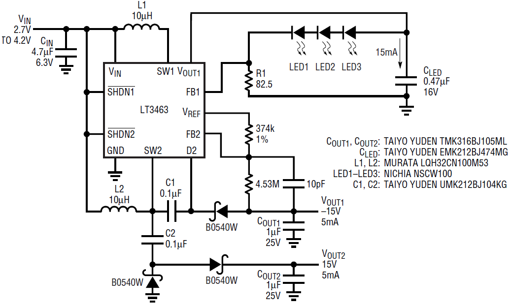
A typical LCD application requires both a positive and a negative voltage to drive the glass and, in some cases, a means of illuminating the back panel. The LT3463 circuit shown in Figure 1 provides all three. The outputs of this circuit are 15V, –15V and a 15mA LED driver. The –15V rail is generated from an inverting charge pump regulated by channel 2 of the LT3463. A quasi-regulated charge pump tapped from the switch node of channel 2 forms the 15V rail. Channel 1 is configured as current source boost converter and supplies current to the LEDs. The advantages offered by this circuit are low quiescent current and minimal parts count.

Figure 1. ±15V converter plus LED driver.
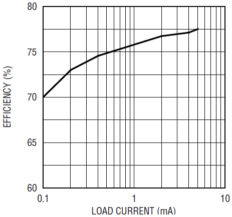
The on-demand power delivery provided by the Burst Mode operation of the LT3463 allows the ±15V rails to have a no-load quiescent current of 76µA and an efficiency of over 73% from 5% load to 100% load for an input voltage of 3.6V. The full load efficiency is 77% at 3.6V. (See Figure 2.) Because a charge pump is used for both the positive and negative output, the load is disconnected from the output during shutdown which increases battery run time. The slave charge pump for the +15V rail does require more parts than a slave boost converter, but the extra parts are offset by the internal Schottky diodes of the LT3463.

Figure 2. Total efficiency of ±15V converter at VIN = 3.6V.
The LED driver is best suited for applications that require only a single level of backlighting or partial dimming. The time constant formed by CLED and R1 does not allow PWM dimming over the entire range of brightness. The LED driver has an efficiency of 76% at an input voltage of 3.6V. During shutdown, less than 1µA flows through the LEDs from VIN.


