How to Generate Auxiliary Supplies from a Positive Buck DC-DC Converter
Abstract
Many applications require a low-power supply in addition to the main supply. For reasons of cost, inventory management, or electromagnetic compatibility (EMC), a separate converter may not be appropriate. Consequently, another means of providing extra power rails from the main supply is needed. This application note shows how to use a step-down IC converter's switching action to derive one or more outputs, isolated or non-isolated, quasi-regulated or unregulated.
Introduction
Many applications require a low-power supply in addition to the main supply. A typical example is when an analog front-end amplifier needs ±5V, while the main digital circuitry requires +5V only. For reasons of cost, inventory management, or EMC, a separate -5V converter may not be appropriate. Consequently, another means of providing extra power rails from the main supply is needed.
As a solution to this problem, a step-down IC converter's switching action can be used to derive one or more outputs, isolated or non-isolated, quasi-regulated or unregulated. Auxiliary output currents of 10% to 30% of the main output are perfectly possible. This application note will illustrate this technique using the MAX5035 DC-DC converter.
Step-Down Waveforms
A review of the waveforms found in a working step-down converter will identify the voltage and currents that can be used to generate additional outputs. See Figure 1 below and Example 1 waveforms at the end of this article.
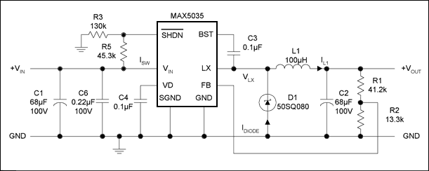
Figure 1. The MAX5035 schematic illustrates step-down converter operation.
There is a switching voltage waveform of amplitude at the LX pin:
VLX = [VIN (max) to -V(diode)] < VLX < VIN(min) -V(diode)]
The voltage across the main inductor during the power cycle (LX connected to VIN) is:
VIND = [VIN (max) - VOUT] < VIND < [VIN(min) - VOUT]
Continuous Inductor Current Operation
When the power switch is off, the voltage at the LX connection flies negative, turning on the diode, D1, to ensure that the inductor current continues to circulate. Operation is said to be continuous when the power cycle begins before the circulating current in D1 falls to zero (Figure 2).
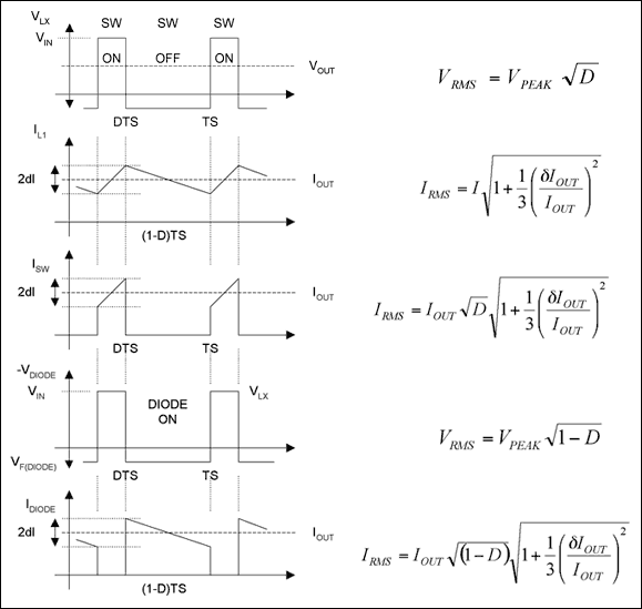
Figure 2. Continuous inductor current waveforms. TS = switching period; D = duty cycle.
Knowing the various RMS currents and voltages associated with the key components, power dissipation can be calculated as follows:

Definitions
RON_SW—Data sheet on-resistance of the internal power switch (VIN to LX)
RLOAD—Effective resistance connected at the power-supply output.
IQUIESCENT—Quiescent current of the control IC with no switching action.
IDIODE_RMS—Schottky diode (D1) forward RMS current.
VFORWARD—Forward voltage drop across Schottky diode, D1, at rated current.
ILOAD_RMS—RMS load current.
Auxiliary Outputs
Auxiliary outputs can be added to the main step-down by an additional winding on its inductor. The additional output relies on flyback action in the main inductor during the time that the 'catch' Schottky diode (D1 in Fig1) is conducting. Because the diode voltage drop is relatively constant (300mV to 500mV, typically, depending on current), and because the controller regulates the output voltage, the inductor's voltage drop is also relatively constant during the OFF time of the power switch. For the voltage drop to remain consistent, the main inductor should be in continuous conduction throughout the main step-down load range.
The LX pin can also be used to provide a switching input to a discrete charge-pump circuit. For this to remain consistent, the LX pin must be active whenever the additional output is required. You can keep the LX pin active by ensuring that the main step-down output supports a minimum load.
Inductor Selection
Three functions are needed to set the value of the main inductor: the voltage across the inductor, the operating frequency, and the inductor's current ripple. Together, these functions will ensure that adequate energy is stored in the inductor. The inductor's minimum value is determined by the maximum duty cycle and minimum input voltage, and is given by:

Ripple current is a percentage of output current, and defined as 30% for the MAX5035. Note that the ripple current sets the minimum load current before the onset of discontinuous operation. Because an auxiliary supply increases the peak-current requirements of the power switch, care must be taken to limit the auxiliary power drawn.
For many applications, the Evaluation (EV) kit's standard setup of 100µH and 68µF output filter values will be suitable. These values are retained for the additional supplies. The MAX5035 features fixed, internal type-3 compensation which imposes limitations on the choice of output capacitor. Chose the ESR so that the zero frequency occurs between 20kHz and 40kHz. See the application section of the MAX5035 data sheet for more information.
Auxiliary Output Derived from the Main Inductor's Transformer
The inductor's voltage drop is relatively constant during the power switch's OFF time, because the primary Schottky diode voltage drop is relatively constant (300mV to 500mV, typically, depending on current), and the controller regulates the output voltage. Connecting the secondary rectifier and capacitor so that conduction occurs during the flyback period (diode ON), allows some energy to be tapped off the main inductor. Figures 3a and 3b show two versions of this arrangement. Isolating the auxiliary winding from the main step-down allows flexible connection arrangements. Figure 3a shows the auxiliary output referred to zero volts, and Figure 3b shows the auxiliary output referred to the main positive output. See also waveforms in Examples 2a and 2b.
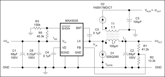
Figure 3a. Transformer serves as the main inductor (auxiliary output referenced to zero volts. T1 = Cooper Bussmann DRQ125-101. (Note the DOT convention for the start of windings.)
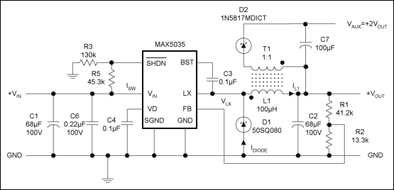
Figure 3b. Transformer as main inductor (+ve auxiliary output referenced to main output). T1 = Cooper Bussmann DRQ125-101. (Note the DOT convention for the start of windings.)
Auxiliary output voltage is given by:
VAUX = N2/N1 (VOUT + VDIODE1) - VDIODE2
N1 = primary turns and N2 = secondary turns.
This output in Figure 3 is independent of input-voltage changes, as D2 is ON when the internal LX power switch is OFF. Capacitor C7 should be chosen to support the output during the maximum on-time of the power switch. The secondary output suffers a 2% to 3% output variation as the forward voltage drop of D1 varies with temperature and load current. Since N1 and N2 of the transformer are DC-isolated from each another, the extra output may be referenced to any DC voltage.
For a given inductor value, secondary power at the auxiliary output is limited by the onset of discontinuous current in the main primary loop. Restated simply, D1 must remain in conduction at the end of the flyback period. At the onset of discontinuous operation, conduction through D1 becomes zero, and the voltage at LX will show the characteristic decaying 'ring' at a frequency determined by the output inductance and the total stray capacitance at the LX node.
Secondary loading causes a change of primary current at the point of transition when the internal LX switches from on to off. This current step shown in Figure 4 is given by:
IXTRA = PSEC (D x VLX)
D = duty cycle
PSEC = secondary power
VLX = peak voltage excursion at LX
In principle, there is much flexibility in the choice of turns ratio. However, in practice, the availability of standard 1:1 transformers with suitable inductance and peak-current values makes this the most popular choice of turns ratio.
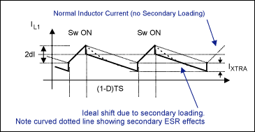
Figure 4. Primary inductor current due to secondary loading.
Note how the additional loading produces changed primary ripple current. Bold lines identify simplified changes to the main-inductor current shape with active auxiliary output.
Relative Advantages of this Approach
- Positive or negative auxiliary output
- Quasiregulated auxiliary output
- Isolated; can be referenced to ground or main positive output
- Inductance value set by main step-down
- Off-the-shelf magnetics (1:1 transformer ratio)
Relative Disadvantages of this Approach
- Increased primary ripple current increases onset of discontinuous current
- Minimum load required on aux output
- Minimum load required on main positive output to maintain switching action at LX
Negative Auxiliary Output Derived from a Charge Pump
The LX terminal voltage excursion can be used as a source for a charge pump to generate an unregulated auxiliary negative output. The additional output is unregulated because the voltage at LX is not isolated from changes of VIN. The additional charge-pump components are shown in Figure 5. See also waveforms in Example 3.
When the power switch closes at the start of the power cycle, current flows into C7 through D2 and R6 and begins to ramp in the inductor, L1. On the flyback cycle when D1 conducts, the charge on C7 is transferred to C8 and the load. R6 is an important addition, as it limits the peak current into C7. Without R6, the current limit of the power switch will be exceeded, causing premature termination of the power cycle and even shutdown on protected step-down converters like the MAX5035. See Figure 6.
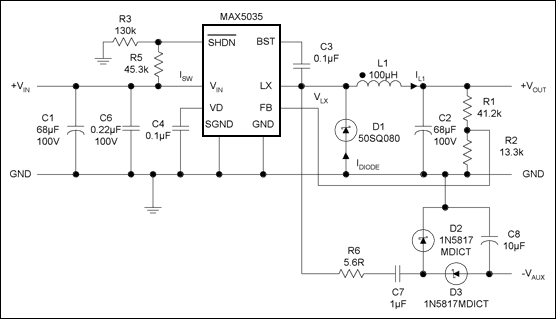
Figure 5. Schematic for an auxiliary negative output derived from a charge pump.
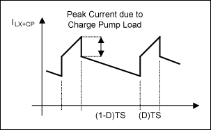
Figure 6. Current waveform from an inductor and charge pump.
The source impedance of the unregulated charge pump due to R6 and C7 is given by:

Identifying the source impedance of the unregulated charge pump allows the designer to estimate the charge-pump output voltage under variable load conditions.
The open-circuit, charge-pump auxiliary output voltage is given approximately by:

The loaded charge-pump auxiliary output voltage is given by:

With capacitor values in the 1µF to 10µF range, R1 will dominate the source impedance. Output ripple is due almost entirely to ESR of C8 (output capacitor in Figure 4). As the charge pump is unregulated, a linear regulator can be connected at the output to provide a regulated negative output.
Relative Advantages of this Approach
- Small components
- Lower cost than 1:1 transformer architecture
Relative Disadvantages of this Approach
- Unregulated output; an additional regulator may be needed at output if the input voltage has a wide range.
- High peak currents for modest auxiliary load currents (approx 4 x IOUT_AVE)
- Negative auxiliary output only; the output can be referenced to ground or the main regulated output, provided that enough voltage difference is available to charge the pump capacitor (C7 in Figure 5).
- Minimum load required on auxiliary output to prevent spike storage overvoltage
- Minimum load required on main positive output to maintain switching action at LX
SEPIC Auxiliary Supply
A negative output can be obtained from the LX pin by employing a second inductor, L2, which shares the same core and, therefore, the same value as the main step-down inductor. Figure 7 shows how C5, D2, C6, and L2 form a SEPIC topology. See also waveforms in Example 4. The switching signal at LX driving the positive-output step-down is also the same level for driving the negative output. During the switch ON period, the voltage across L1 is VLX - VOUT, and during the OFF period is VOUT + VDIODE_1). By transformer action (1:1) this voltage is also impressed across L2 and generates -VOUT with D2 and C5. Because of the less-than-perfect coupling of the two windings L1 and L2, C5 creates the SEPIC connection and improves regulation of what would be a normal flyback auxiliary output with very modest regulation.
The coupling capacitor, C5, is chosen to produce a low-voltage ripple across it as a function of auxiliary load-current duty cycle and clock period.

Relative Advantages of this Approach
- Quasiregulated output
- 'Clean' inductor current waveform; less noise generation
- Ripple reduction due to coupled inductors
- Single magnetic component (off-the-shelf 1:1 transformer)
Relative Disadvantages of this Approach
- -VOUT only available
- Ground referenced output
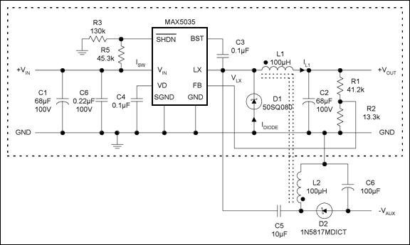
Figure 7. Coupled inductor SEPIC auxiliary supply. L1, L2 = Cooper Bussmann DRQ125-101. (Note the DOT convention for the start of windings.)
Conclusions
A number of auxiliary output topologies can be added to an integrated, positive step-down converter. The MAX5035 was chosen for the examples, but the lower output MAX5033 can employ the same circuits, but at reduced outputs.
Flyback Auxiliary
For complete independence from auxiliary output reference, the flyback circuit adds a winding to the main step-down inductor, a Schottky diode, and a capacitor. This design is very appealing and comes with modest regulation. With a 1:1 transformer (Cooper Bussmann DRQ125-101 for the MAX5035), the auxiliary output can be ±VOUT with respect to ground or the main VOUT. Auxiliary output current can be up to 20% of the main output, although some distortion of the main inductor current is to be expected.
Coupled Inductor SEPIC Auxiliary
Not as versatile in grounding arrangements, the coupled inductor SEPIC topology provides a regulated -VOUT referenced to ground only. Regulation is better than the flyback approach, and inductor current waveform distortion is small. Auxiliary output current can be up to 20% of the main output. The coupled inductor aids ripple reduction in the auxiliary output.
Charge Pump Inverter
The charge pump is the lowest cost option with no additional inductor winding. This design is suitable for low-power outputs only because of the high peak currents and voltages associated with the topology. Open-circuit output is approximately VIN, reducing as the loading is increased on the auxiliary output. Suggested maximum loading is 5% or less of the main positive output.
With this approach the main positive output must remain active at all times, and the main step-down inductor current must remain continuous at all times. Extra peak current will be demanded by the auxiliary output, and this must be taken into account when minimum loading of the main output and maximum loading of the auxiliary output are considered.
| Supplier | Component | Website |
| AVX Ceramic | capacitors | www.avx.com/ |
| Coilcraft | Power inductors | www.coilcraft.com |
| Coiltronics | Power inductors | www.cooperET.com |
| Diodes Incorporated | Schottky diodes | www.diodes.com |
| Panasonic | Ceramic/Al capacitors | www.panasonic.com |
| TDK | Ceramic capacitors | www.component.tdk.com |
| Vishay | Diodes, resistors, capacitors | www.vishay.com |
| On-Semiconductor | Schottky diodes | www.onsemi.com |
Example 1 Waveforms: Step-down converter, MAX5035 EV Kit No Auxiliary (Figure 1):
VIN = +15V
VOUT = +5V
IOUT = 465mA (RLOAD = 10Ω ±5%)
Waveforms:
- LX inductor current ramp (Yellow, 0.1A / sq)
- LX voltage (Green)
- VOUT (Violet)
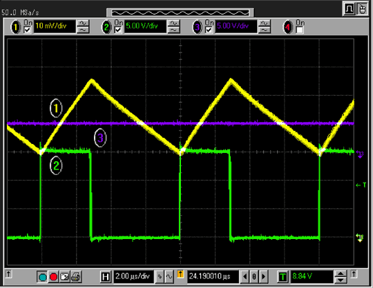
ILX_PEAK = 550mA
VLX_PEAK = 15V
Period = 8µs
Example 2a Waveforms: Transformer as Main Inductor, Flyback Auxiliary Output (Figure 3):
VIN = +15V
VOUT = +5V
IOUT = 465mA (RLOAD = 10Ω µ5%)
-VOUT = 5.02V
-IOUT_AUX = -152mA (RLOAD = 33Ω)
C3 = 100µF
D2 = 1N5817MDICT
Waveforms:
- LX inductor current ramp (Yellow, 0.1A / sq)
- LX voltage (Green)
- VOUT_AUX (Violet)
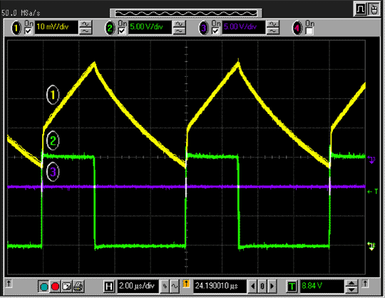
ILX_PEAK = 0.63A
Note: The LX waveform distortion is caused by additional loading during the flyback (D1 ON) period.
Example 2b Waveforms: Transformer as Main Inductor, Flyback Auxiliary Output (Figure 3):
VIN = +15V
VOUT = +5V
IOUT = 465mA (RLOAD = 10Ω µ5%)
-VOUT = 5.3V
-IOUT_AUX = -104mA (RLOAD = 51Ω)
C3 = 100µF
D2 = 1N5817MDICT
Waveforms:
- LX inductor current ramp (Yellow, 0.1A / sq)
- LX voltage (Green)
- VOUT_AUX (Violet)
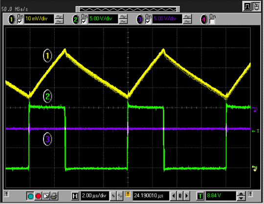
ILX_PEAK = 0.6A
Note: the reduced LX waveform distortion is caused by reduced loading on flyback (D1 ON) period. Compare this to Example 2a above.
Example 3 Waveforms: Charge Pump Negative Auxiliary Output (Figure 5):
VIN = +15V
VOUT = +5V
IOUT = 465mA (RLOAD = 10Ω µ5%)
-VOUT = -12.3V
-IOUT_AUX = 82mA (RLOAD = 150Ω
D2, 3 = 1N5817MDICT
C7 = 1µ
C8 = 10µF
R6 = 5.6Ω
Waveforms:
- LX + Charge Pump current ramp (Yellow, 0.2A / sq)
- LX voltage (Green)
- -VOUT_AUX (violet, 500mV / sq), AC-coupled.
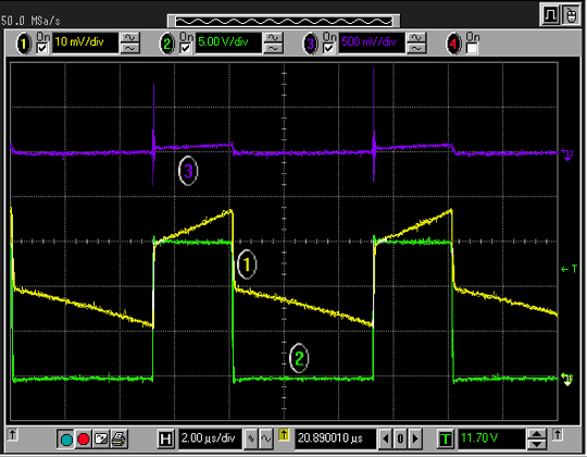
Lx current waveform = 750mA pk. Contrast with 550mA peak of the basic step down.
Note: the dV/dT spikes at auxiliary output. Post filter with small LC. L may be formed from pc copper track.
Example 4 Waveform: SEPIC Auxiliary Supply (Figure 7):
L1 = L2 = 100µH coupled (1:1) inductor
VIN = +15V
VOUT = +5V
IOUT = 465mA (RLOAD = 10Ω µ5%)
-VOUT = -5.02V
-IOUT_AUX = 228mA (RLOAD = 22Ω)
C5 = 10µF
C6 = 100µF
D2 = 1N5817MDICT
Waveforms:
- LX current ramp (Yellow, 0.2A / sq)
- LX voltage (Green)
- VOUT_AUX (Violet)
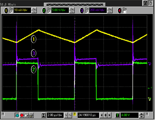
ILX_PEAK = 1.15A
VOUT_AUX Ripple = 100mV pk-pk excluding narrow dV/dT pulses.
Note: dV/dT spikes at auxiliary output. Post filter with small LC. L may be formed from pc copper track.

