The Harsh Reality of Wide-Ranging 4V–36V Automotive Batteries Is No Problem for Triple Output Regulator in 4mm × 5mm QFN
The Harsh Reality of Wide-Ranging 4V–36V Automotive Batteries Is No Problem for Triple Output Regulator in 4mm × 5mm QFN
Jul 1 2011
DC/DC converters for automotive applications must operate in an environment of extremes. Input transients can exceed the nominal battery voltage by a factor of five and last hundreds of milliseconds, while temperatures under the hood soar far above the capability of typical commercial grade ICs. In this harsh environment, space is tight, so even the most robust devices must perform multiple functions.
The LT3694/LT3694-1 meets these requirements by combining a 2.6A switching regulator and two low dropout linear regulators in a compact 4mm × 5mm QFN package or a thermally enhanced TSSOP. The switching regulator requires a single inductor and has an internal power switch, cycle-by-cycle current limiting and track/soft-start control. Each LDO requires only an external NPN pass transistor and includes foldback current limiting and track/soft-start control. An internal overvoltage detector shuts off the switching regulator when VIN exceeds 38V, protecting the switch and the Schottky rectifier. This allows it to survive transients on VIN up to 70V without damage to itself or the rectifier.
4V–36V Input Switching Regulator
The LT3694/LT3694-1 includes a 36V monolithic switching regulator capable of providing up to 2.6A of output current from input voltages down to 4V. Output voltages can be set as low as the feedback reference of 0.75V.
The regulator uses a current mode, constant frequency architecture, which keeps loop compensation simple. External compensation allows custom tailoring of loop bandwidth, transient response and phase margin.
Two Low Dropout Linear Regulators
The LT3694/LT3694-1 includes two LDO linear regulators that use an external NPN pass transistor to provide up to 0.5A of output current. The base drive can supply up to 10mA of base current to the pass transistor and is current limited. The LDO is internally compensated and is stable with output capacitance of 2.2µF or greater. It uses the same 0.75V feedback reference as the switching regulators.
The LDO drive current is drawn from the BIAS pin if it is at least 0.9V higher than the DRIVE pin voltage, otherwise it’s drawn from VIN. This reduces the power consumption of the LDO, especially when VIN is relatively high.
The LDO has foldback current limiting by monitoring a sense resistor in the collector of the NPN pass transistor. The initial threshold is set at 60mV, but folds back as VFB decreases until at VFB = 0 the threshold is at 26mV. A sense resistor of 0.1Ω sets the operating current limit at 600mA, but the short circuit current limit drops to 260mA. This reduces power dissipation in the pass transistor with a shorted output.
The LDOs can be shut down by pulling the FB pin above 1.25V with at least 30µA. If independent control of the LDOs is needed, each LDO output can be forced to 0V by pulling its TRK/SS pin low. If the track or soft-start functions are needed, use an open drain output in parallel with the track or soft-start circuitry described below. If track and soft-start are not necessary, then a standard CMOS output (from 1.8V to 5V) with a 1k series resistor works fine.
Track/Soft-Start Control
The buck regulator and each LDO has its own track/soft-start (TRK/SS) pin. When this pin is below the 0.75V reference, the regulator forces its feedback pin to the TRK/SS pin voltage rather than the reference voltage. The TRK/SS pin has a 3µA pull-up current source.
The soft-start function requires a capacitor from the TRK/SS pin to ground. At startup, this capacitor is at 0V, which forces the regulator output to 0V. The current source slowly charges the capacitor voltage up and the regulator output ramps up proportionally. Once the capacitor voltage reaches 0.75V, the regulator locks onto the internal reference instead of the TRK/SS voltage. The TRK/SS pin is pulled low on any shutdown event (overvoltage, overtemperature, undervoltage) in order to discharge the soft-start capacitor.
The track function is achieved by connecting the slave regulator’s TRK/SS pin to a resistor divider from the master regulator output. The master regulator uses a normal soft-start capacitor as described above to generate the start-up ramp that controls the other regulators. The resistor divider ratio sets the type of tracking, either coincident (ratio equal to slave feedback divider ratio) or ratiometric (ratio equal to master feedback divider ratio plus a small offset). The TRK/SS pins can also be tied together to a single capacitor to provide ratiometric tracking, but only if the LDOs are not shut down by pulling FB high (see the section “Two Low Dropout Linear Regulators” above).
Enable and Undervoltage Protection
The LT3694/LT3694-1 includes an enable and user programmable undervoltage lockout function using the EN/UVLO pin. The undervoltage lockout can protect against pulse stretching. It can also protect the input source from excessive current since the buck regulator is a constant power load and draws more current when the input source is low. The undervoltage lockout shuts off all three regulators when tripped.
These two functions use a pair of built-in comparators at the EN/UVLO input. The enable comparator has a 0.5V threshold and activates the internal bias circuits of the LT3694/LT3694-1. When EN/UVLO is below the enable threshold, the LT3694/LT3694-1 is in shutdown and draws less than 1µA with 12V input. The undervoltage comparator has a 1.2V threshold and has 2µA of hysteresis. The UVLO hysteresis is a current sink that activates when EN/UVLO drops below the 1.2V threshold. A resistor divider from VIN to the EN/UVLO input sets the trip voltage and hysteresis. The undervoltage threshold is accurate over temperature to allow tight control over the trip voltage. The EN/UVLO pin should be connected to VIN if the function isn’t used.
Frequency Control
The switching frequency is adjustable from 250kHz to 2.5MHz, set by a single resistor to the RT pin. Higher frequencies allow smaller inductors and capacitors, but use more power and have a smaller allowable step-down range due to the minimum on and off time constraints.
This brings us to the difference between the LT3694 and the LT3694-1. The LT3694 switching frequency can be synchronized to an external clock by connecting it to the SYNC pin. The resistor on the RT pin should be set provide a free running frequency 20% below the sync frequency. The LT3694-1 replaces the SYNC pin with a CLKOUT pin, allowing the LT3694-1 to be used as the master clock for synchronizing other switching regulators. The CLKOUT produces a clock signal running at ~50% duty cycle.
Triple-Output Converter with Voltage Tracking
Figure 1 shows a wide input range, 6.3V to 36V, converter that generates three outputs: 5V, 3.3V and 2.5V. The outputs track ratiometrically, set via a common TRK/SS connection. Figure 2 shows the start-up waveforms of the three outputs along with the enable signal.
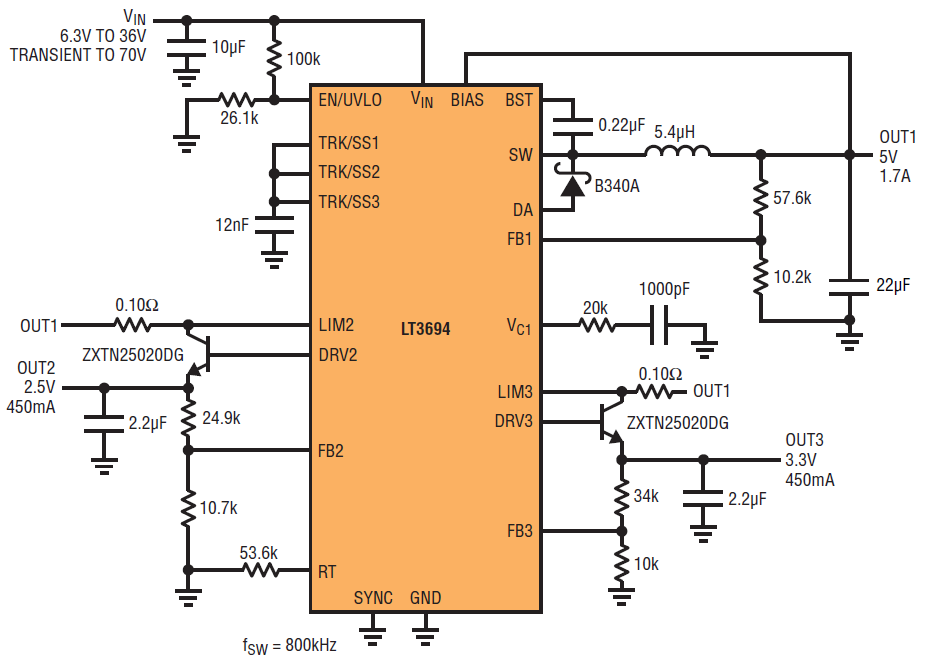
Figure 1. The LT3694/LT3694-1 in a wide input range, triple output application.
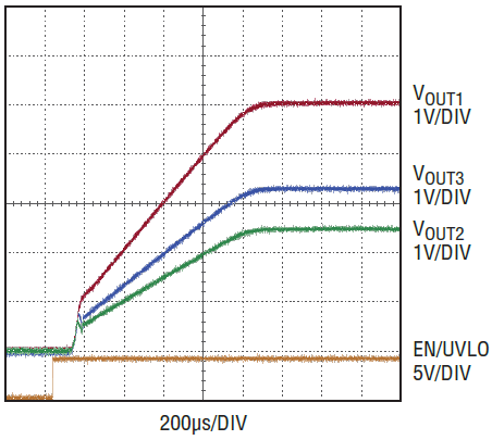
Figure 2. Ratiometric tracking waveforms.
Figure 3 shows the switching regulator efficiency at different input voltages.
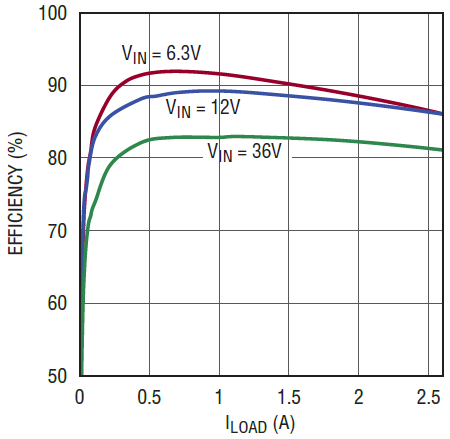
Figure 3. Switching regulator efficiency.
Conclusion
The LT3694/LT3694-1 offers robust, compact power supply solutions by squeezing three regulators into a tiny 4mm × 5mm QFN or a 20-lead TSSOP package. One regulator is an efficient switching regulator and the other two are low noise, low dropout linear regulators. Just a few small external components are needed to create an extremely compact triple output solution.
About the Authors
Michael Nootbaar joined Analog Devices Inc. as a senior design engineer, part of the founding team of the company’s Grass Valley, CA design center in 2003. He has designed and released numerous integrated circuits in the a...


