Designing to Protect MAX2140's Internal ESD Diode During Nonstandard Operation *
Abstract
The MAX2140 SDARS receiver can experience internal ESD diode failure during a hot-plug operation (connection or disconnection with power applied), which is not a standard operation for this device. While this can occur in many applications, hot-plugging is a high probability in the automotive industry. This article reviews the cause of the ESD diode problem during hot-plug, and helps calculate and properly design the circuitry to prevent the failure.
Introduction
There are conditions during assembly, testing, and troubleshooting which require nonstandard performance from the MAX2140 SDARS receiver. One such example is a 'hot plug'—the connection or disconnection of the circuitry containing the device while power is applied. Hot-plug is, especially common in the automotive industry where the modular design of components, the distance between the modules, and the numerous systems working simultaneously require reconnecting modules.
How a Hot-Plug Operation Can Cause Diode Failure
Hot-plugging causes transients, which are characterized by significant voltage, current surges, ringing, and the swap of polarity. The physics behind the transient processes include energy exchange, finite charging/discharging time, and self-resonance.
Figure 1 illustrates a common hot-plug operation for the MAX2140.
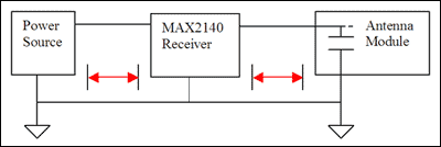
Figure 1. Illustration of a common usage of the MAX2140 in the automotive industry.
During a hot-plug event, voltage drops (shown as red arrows on the drawing) will accrue on the interface cables. Simultaneously, the bypass capacitor inside the antenna module acts as an electrical short. As a result, the MAX2140's electrical ground rises above the electrical ground of the antenna module. This difference creates for a short time a forward voltage on the MAX2140's internal ESD diode, which is connected from the IC's ground to pin 16. That forward voltage spike can exceed the device's absolute maximum ratings, and is known as Electrical Overstress (EOS). The diode's forward voltage is specified at -0.3V to +4.3V (VCC_xx to GND; VINANT to GND; AGCPWM to GND; VOUTANT to GND). Design simulation shows that -1.3V at 72mA is possible for short-term operation.
Designing to Prevent ESD Diode Failure
The best method for preventing EOS will vary with your application. Some common recommended design modifications follow:
- Avoid use of too much reactance: storage, bypass capacitors; RF noise choke inductors; long interfaces.
- Reroute surge currents: provide a short, solid ground to each module; add external diodes in parallel with internal diodes; put diodes across large coils.
- Sequence power supplies (if possible): turn on power supplies in sequence; introduce programmable delays to internal users. (Analog has an extensive line of power supply sequencing products.)
The following design example (Figure 2) shows the MAX2140 with local grounding and a Schottky diode added to provide adequate bypass for the current surge.

Figure 2. Diagram of the design modifications between the MAX2140 receiver and antenna module. The modifications will prevent EOS.
Specific design modifications are:
- The cable between the MAX2140 receiver and antenna module has 0.5Ω resistance and no inductance.
- The antenna module has a 100µF bypass capacitor.
- The MAX2140 receiver supplies 5V to the antenna module.
One can now reasonably ask, what is the maximum current through the capacitor and voltage drop across the cable during the first 40µs transient? These values can be determined from the following equation:

This equation calculates the momentary current through the capacitor, where du and dt can be replaced by delta values accordingly. Here C is the value of the capacitor.

Where the capacitor will be charged from 0V to 5V.

Which represents the time interval between 0 to 40µs.
The current through the bypass capacitor can be represented by:

The voltage drop across the cable during the 40µs transient is:

As an example, the voltage could be 6.25V at 12.5A, which greatly exceeds the short-term requirements for the internal ESD diode. Adding an Schottky diode will bypass most of the current surge during the transient. A generic Schottky diode for pulse applications is a good candidate for this task. Based on the design in Figure 2 above, a short cable will significantly reduce resistance and voltage drop, while using a reasonable capacitor value will reduce the maximum current surge to an acceptable level.
Conclusion
There are ways to accommodate nonstandard usage of a device, such as hot-plug operation of the MAX2140 receiver. To be successful, the process requires careful design and proper testing of the product, along with Maxim's support and approval.
* Stresses beyond 'Absolute Maximum Ratings' can cause permanent damage to the device. These absolute maximum ratings are stress ratings only. Functional operation of the device at this, or any other conditions beyond those indicated in the operational specifications is not implied. Exposure to absolute-maximum-rating conditions for extended periods can affect device reliability.


