Chip Scale Packaging Helps Portable Medical Devices Save Size and Weight
Chip Scale Packaging Helps Portable Medical Devices Save Size and Weight
Dec 1 2010
Wafer-level chip scale packages are allowing designers of portable healthcare equipment—such as invasive sensing, medical implants, and disposable monitors—to reduce size and power requirements.
One of the key trends in medical equipment design is to bring equipment closer to patients at the doctor’s office or at their own home by making these devices more portable. This involves all aspects of the design, but especially effects size and power consumption. Shrinking the electronic portion of these instruments is being aided greatly by the use of wafer-level chip-scale packages (WLCSPs).
These new applications include invasive sensing, medical implants, and disposable, portable monitors. But to get the most out of WLCSPs in terms of performance and reliability, designers should heed the best practices in designing the printed-circuit board (PCB) land pattern, pad finish, and board thickness.
Wafer-level chip scale packaging is a variant of the flip-chip interconnection technique (Figure 1). With WLCSPs, the active side of the die is inverted and connected to the PCB using solder balls. The size of these solder balls is typically large enough (300 µm pre-reflow for 0.5-mm pitch, and 250 um pre-reflow for 0.4-mm pitch) to avoid the underfill that is required for flip-chip interconnects. This interconnection technology offers several advantages.
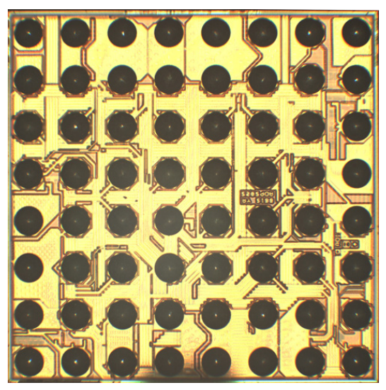
Figure 1. WLCSP Package
First, considerable space savings are obtained by eliminating the first level package (mold compound, lead frame, or organic substrate). For example, an 8-ball WLCSP occupies only 8% of the board area taken up by an 8-lead SOIC. Next, inductance is reduced and electrical performance is improved by eliminating the wire bonds and leads used in standard plastic packages.
Also, designs yield a lighter weight and thinner package profile, due to the elimination of the lead frame and molding compound. No underfill is required, as standard surfacemount (SMT) assembly equipment can be used. And finally, high assembly yields result from the self-aligning characteristic of the low mass die during solder attachment.
Package Construction
WLCSPs can be categorized into two construction types: direct bump and redistribution layer (RDL).
A direct-bump WLCSP consists of an optional organic layer (polyimide), which acts as a stress buffer on the active die surface. The polyimide covers the entire die area except for openings around the bond pads. An under-bump metallurgy (UBM) layer is sputtered or plated over this opening. The UBM is a stack of different metal layers serving as diffusion layer, barrier layer, wetting layer, and antioxidation layer. The solder ball is dropped (which is why it's called ball-drop) over the UBM and reflowed to form a solder bump (Figure. 2).
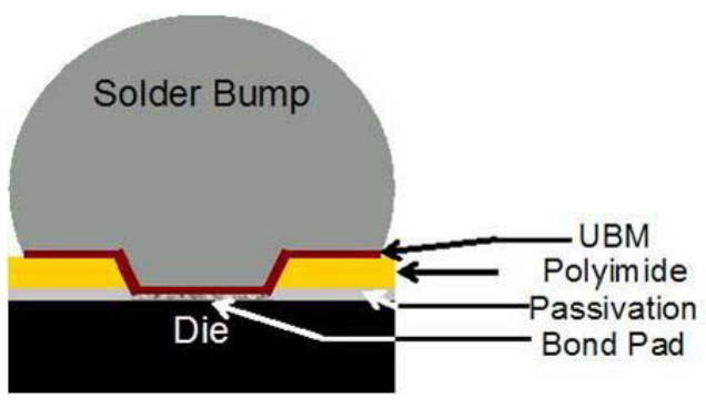
Figure 2. Direct Bump WLCSP
RDL technology allows a die designed for wire bonding (with bond pads arranged along the periphery) to be converted into a WLCSP. In contrast to a direct bump, this type of WLCSP uses two polyimide layers. The first polyimide layer is deposited over the die, keeping the bond pads open. An RDL layer is sputtered or plated to convert the peripheral array to an area array. The construction then follows the direct bump, with a second polyimide layer, UBM, and ball drop (Figure 3).

Figure 3. Redistribution Layer (RDL) WLCSP
Post ball-drop are wafer backgrind, laser-marking, testing, singulation, and tape and reel. There is also an option of applying a backside laminate after the backgrinding process to reduce die chipouts induced during sawing and to ease the handling of the package.
Best PCB Design Practices
The critical board design parameters are pad opening, pad type, pad finish, and board thickness. Based on the IPC standard, the pad opening equals the UBM opening. The typical pad openings are 250 µm for a 0.5-mm pitch WLCSP and 200 µm for a 0.4-mm pitch WLCSP (Figure 4).
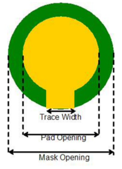
Figure 4. Pad Opening
The solder mask opening is 100 µm plus the pad opening. The trace width should be less than two-thirds of the pad opening. Increasing the trace width can reduce the stand-off height of the solder bump. Hence, maintaining the proper trace width ratio is important to ensure the reliability of the solder connections. For board fabrication, two types of pads/land patterns are used for surface-mount assembly (Figure 5):
- Non-solder-mask defined (NSMD): The metal pad on the PCB (to which the I/O is attached) is smaller than the solder-mask opening.
- Solder-mask defined (SMD): The solder-mask opening is smaller than the metal pad

Figure 5. Pad Type
Because the copper etching process has tighter control than the solder-mask opening process, NSMD is preferred over SMD. The solder-mask opening on NSMD pads is larger than the copper pads, allowing the solder to attach to the sides of the copper pad and improving the reliability of the solder joints.
The finish layer on the metal pads has a significant effect on assembly yield and reliability. The typical metal pad finishes used are organic surface preservative (OSP) and electroless nickel immersion gold (ENIG). The thickness of the OSP finish on a metal pad is 0.2 µm to 0.5 µm. This finish evaporates during the reflow soldering process, and interfacial reactions occur between the solder and metal pad.
The ENIG finish consists of 5 µm of electroless nickel and 0.02 µm to 0.05 µm of gold. During reflow soldering, the gold layer dissolves rapidly, followed by reaction between the nickel and solder. It is extremely important to keep the thickness of gold below 0.05 µm to prevent the formation of brittle intermetallic compounds. Standard board thicknesses range from 0.4 mm to 2.3 mm. The thickness selected depends on the required robustness of the populated system assembly. The thinner board results in smaller shear stress range, creep shear strain range, and creep strain energy density range in the solder joints under the thermal loading. Hence, the thinner buildup board would lead to a longer thermal fatigue life for solder joints.
Testing and Assessment
In conjunction with the aforementioned variables, WLCSP reliability is assessed by subjecting the device to accelerated stress tests such as high temperature storage (HTS), highly accelerated stress testing (HAST), autoclave testing, temperature cycling, high temperature operating life testing (HTOL), and un-biased highly accelerated stress testing (UHAST). In addition to thermo-mechanical induced stress testing, mechanical tests such as drop and bend testing are also carried out.
HTS testing is performed to determine the effect of longterm storage on devices at elevated temperatures without any electrical stresses applied. This test assesses the long-term reliability of devices under high temperature conditions. The typical test conditions are 150°C and/or 175°C for 1000 hours. This test consists of exposing the parts at the specified ambient temperature for a specified amount of time.
Resources
For further information on healthcare applications, visit www.analog.com/healthcare.


