Accurate and Fast 80MHz Amplifier Draws only 2mA
Introduction
The 80MHz LT1800 amplifier consumes a mere 2mA max supply current and still provides both the speed and DC accuracy required by low voltage signal conditioning and data acquisition systems. Usually, one cannot have both high bandwidth and low supply-current in an amplifier, but the LT1800 optimizes both through a 6GHz fT process and by running the transistors at reduced quiescent currents. It can operate from supplies as low as 2.5V, and the entire supply range is available because of the device’s rail-to-rail inputs and outputs. The DC performance is exceptional, with a maximum offset voltage of 350µV. This comes from trimming the input offset voltage, and canceling the input bias currents, where the maximum input bias current is 250nA. The device is available in commercial and industrial temperature grades, in both SOIC and SOT-23 packages, making for a tiny and versatile amplifier.
Performance
Table 1 summarizes the performance of the LT1800. The input offset voltage and input bias current are specified and guaranteed with the common mode voltage at each rail. Both input offset voltage and input bias current are trimmed for maximum accuracy with the inputs near the negative rail.
| Parameter | Conditions | Value | Units |
| –3dB Bandwidth | AV =1 | 80 | MHz |
| Gain-Bandwidth Product | 80 | MHz | |
| Slew Rate | 25 | V/μs | |
| Supply Current | 2.0 Max | mA | |
| Operating Supply Range | 2.5 to 12 | V | |
| Input Offset Voltage | VCM = 0V, SO-8 | 350 Max | μV |
| VCM = 0V, SOT-23 | 750 Max | ||
| VCM = V+, SO-8 | 3000 Max | ||
| VCM = V+, SOT-23 | 3500 Max | ||
| Input Bias Current | VCM = 1V | 250 Max | nA |
| VCM = V+ | 1500 Max | ||
| CMRR | VS = 5V, VCM = 0V to 3.5V | 85 Min | dB |
| PSRR | VS = 2.5V to 10V, VCM = 0V | 80 Min | dB |
| Input Voltage Noise | f = 10kHz | 8 | nV/√Hz |
| Harmonic Distortion | fC = 1MHz, VS = 5V, AV =1, VO = 2VP–P | –75 | dBc |
| AVOL | VS = 5V, VO = 0.5V to 4.5V, RL =1k | 35 Min | k |
| Output Voltage Swing HIGH | IL = 5mA | V+ – 250 Max | mV |
| IL = 20mA | V+ – 750 Max | ||
| Output Voltage Swing LOW | IL = 5mA | 160 Max | |
| IL = 20mA | 450 Max |
The LT1800 is well behaved with capacitive loading, making it easier to use than most other 80MHz amplifiers. Figures 1 and 2 show the small signal behavior of the device with a 1k load, and with 1k in parallel with 50pF. The large signal response is also well behaved, as can be seen in Figure 3.
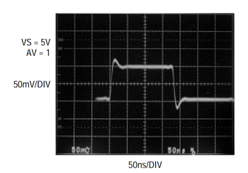
Figure 1. Small signal response RL = 1k.
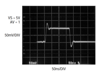
Figure 2. Small signal response RL = 1k, CL = 50pF.
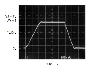
Figure 3. Large signal response RL = 1k, CL = 50pF.
Circuit Description
Figure 4 shows a simplified schematic of the amplifier. The circuit is composed of three distinct stages: an input stage, an intermediate stage, and an output stage. The input stage consists of two differential amplifiers, a PNP stage (Q1-Q2) and an NPN stage (Q3-Q4), that are active over different portions of the input common mode range. The intermediate stage is a folded cascode configuration formed by Q12-Q16, which provides most of the voltage gain. A pair of complementary common emitter devices, Q17-18, creates an output stage which can swing from rail to rail.
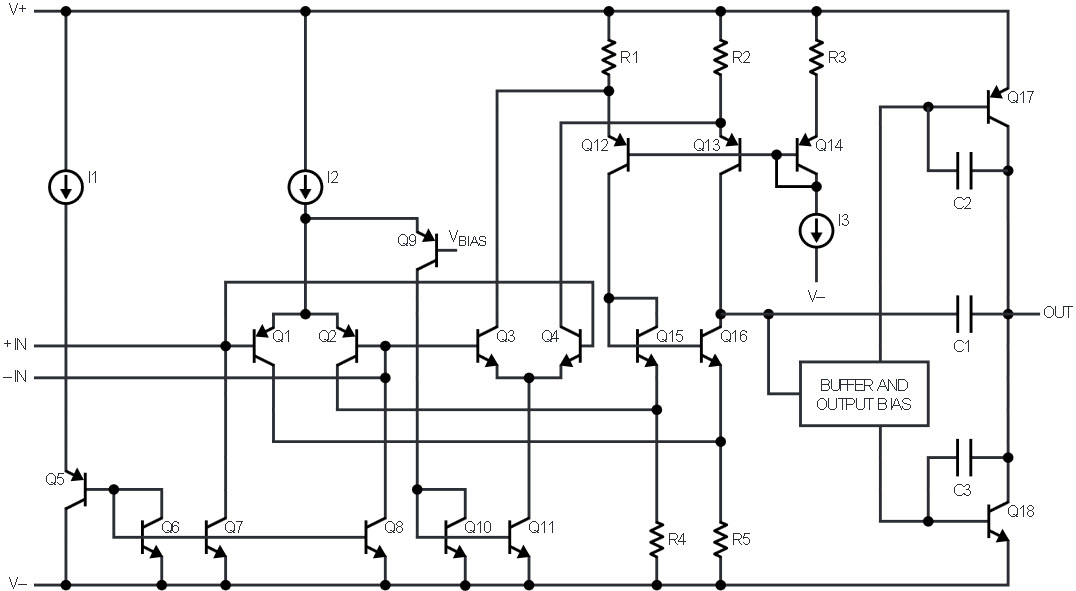
Figure 4. Simplified schematic.
Looking at the input stage, devices Q5-8 act to cancel the bias current of the PNP input pair. When Q1-Q2 are active, the current in Q5 is controlled to be the same as the current in Q1-Q2, thus the base current of Q5 is nominally equal to the base current of the input devices. The base current of Q5 is mirrored by devices Q6-Q8 to each input. The cancellation is effective for common mode voltages greater than the saturation voltage of Q7 and Q8, about V– + 0.2V, up to the voltage that the PNP devices switch off, about V+ – 1.2V.
1MHz 4th Order Butterworth Filter for 3V Operation
The circuit shown in Figure 6 makes use of the low voltage operation and the wide bandwidth of the LT1800 to create a DC accurate 1MHz 4th order lowpass filter powered from a 3V supply. The amplifiers are configured in the inverting mode for the lowest distortion and the output can swing rail-to-rail for maximum dynamic range. Figure 7 displays the frequency response of the filter. Stopband attenuation is greater than 100dB at 50MHz. With a 2.25VP–P, 250kHz input signal, the filter has harmonic distortion products of less than –85dBc. Worst-case output offset is less than 6mV.

Figure 6. 3V, 1MHz, 4th order Butterworth filter.
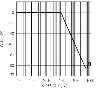
Figure 7. 1MHz filter frequency response.
Fast 1A Current Sense
Figure 8 shows a simple, fast current sense suitable for quickly responding to out of range currents. The configuration amplifies the voltage across the 0.1Ω sense resistor by a gain of 20, resulting in a conversion gain of 2V/A. The –3dB bandwidth of the circuit is 4MHz, and the uncertainty due to VOS and IB is less than 4mA. The minimum output voltage is 60mV maximum, corresponding to 30mA. Figure 9 shows the large signal response of the circuit.
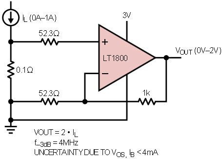
Figure 8. Fast 1A current sense.
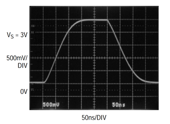
Figure 9. Current sense amplifier large signal response.
Single Supply 1A Laser Driver
Figure 10 shows the LT1800 used in a 1A laser driver application. One of the reasons the LT1800 is well suited to this control task is that its 2.4V operation ensures that it will be awake upon power-up and in control before the circuit can otherwise cause significant current to flow in the 2.1V threshold laser. Driving the noninverting input of the LT1800 to some voltage VIN causes its output to rise, turning on the FMMT619 high current NPN transistor and the SFH495 IR laser. The transistor and laser will turn on until the input voltage appears back at the LT1800 inverting input, and therefore also appears across the 1Ω resistor R1. In order for this to occur, a current equal to VIN/R1 must exist, and the only place it can come from is through the laser. The overall circuit is therefore a V-to-I converter with a 1 ampere per volt characteristic.
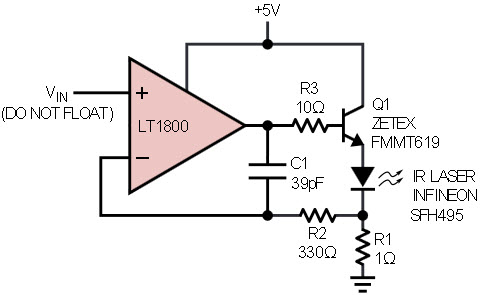
Figure 10. Small 1A low duty cycle laser driver.
Lower values for R1 may be selected, but the designer is reminded to keep series loop traces very short: for example, even 10nH of lead inductance will cause a 16MHz pole into 1Ω, and a 1.6MHz pole into 0.1Ω! Also, when decreasing the value of R1, consider the total of the dynamic impedances of the transistor VBE and the laser. They divide the feedback voltage by R1 thus increasing circuit noise gain. This has the effect of degrading the DC precision and reducing the achievable bandwidth.
Frequency compensation components R2 and C1 were selected for fast but zero-overshoot time domain response, to avoid overcurrent conditions in the laser. They may vary from design to design depending on desired response characteristics, circuit layout, the value of R1, and the actual laser and transistor devices selected. Although not found to be absolutely necessary, R3 is included to ensure a minimum linear load for the op amp. Figure 11 shows the time domain response of this circuit, measured at R1, and given a 500mV 230ns input pulse. While the circuit shown is capable of 1A operation, the laser and the transistor are thermally limited and so must be operated at low duty cycles.
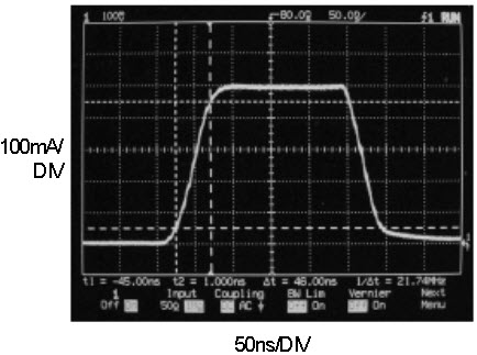
Figure 11. Pulse response of 1A laser driver circuit shows better than 50ns rise time on 500mA pulse.
Low Power High Voltage Amplifier
Certain recently developed materials have optical characteristics that depend on the presence and strength of a DC electric field. Many applications for these materials require a bias voltage applied across the materials, sometimes as high as 100s of volts, precisely in order to achieve and maintain desired properties in the material. The materials are not conductive, and present an almost purely capacitive load.
Figure 12 shows the LT1800 used in an amplifier intended for capacitive loads and capable of 250V output swing. When no input signal is present, the op amp output sits at about mid-supply. Transistors Q1 and Q3 create bias voltages for Q2 and Q4, which are forced into a low quiescent current by degeneration resistors R4 and R5. When a transient signal arrives at VIN, the op amp output jumps away from mid-supply and causes current through Q2 or Q4 depending on the signal polarity. The current, limited by the clipping of the LT1800 output and the 3kΩ of total emitter degeneration, is level shifted to the high voltage supplies and mirrored into the capacitive load. This causes a voltage slew at VOUT until the feedback loop (through R3) is satisfied. The LT1800 output then returns back to near mid supply, providing just enough DC output current to maintain the output voltage across R3. The circuit thus alternates between a low current hold state and a higher transient but limited current slew state.
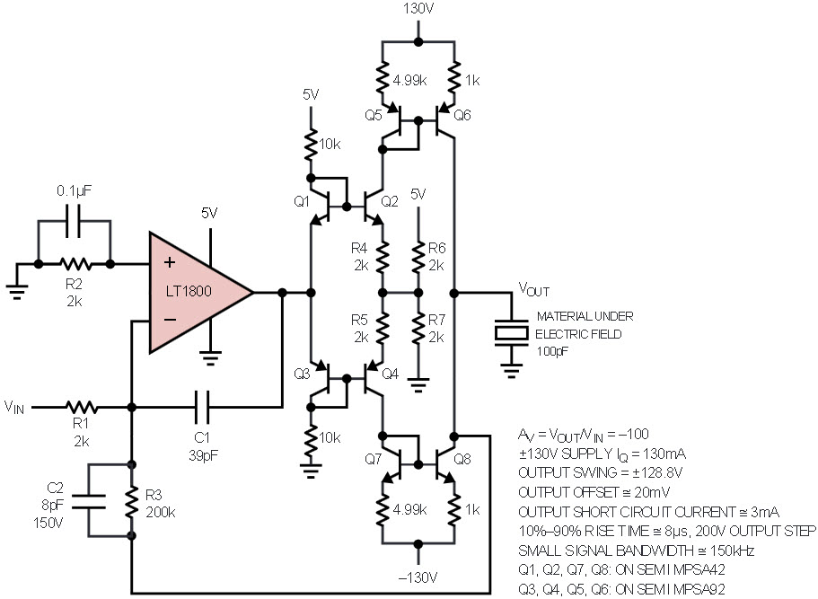
Figure 12. Low power high voltage amplifier.
Careful attention to current levels minimizes power dissipation allowing for a dense component layout, and also provides inherent output short circuit protection. To further save power, the LT1800 is operated single supply with its inputs at ground. Because the inputs are at ground, the LT1800 turns off its internal bias current cancellation, and adding R2 externally restores input precision.
Figure 13 shows the time domain response of the amplifier providing a 200V output swing into a 100pF load.
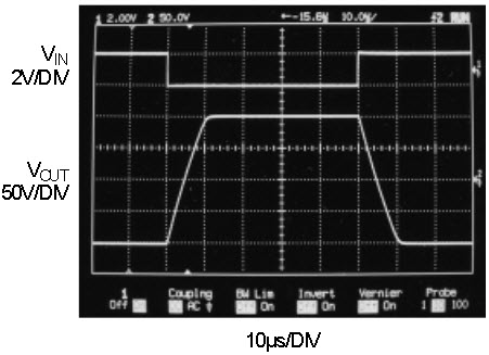
Figure 13. Large signal time domain response of the material bias amplifier.
Conclusion
The LT1800 provides a low power solution to high speed, low voltage signal conditioning. The rail-to-rail inputs and output of the device maximize dynamic range, and can simplify designs by eliminating the negative supply. Circuits that require source impedances of 1k or more, such as filters, will benefit from the low input bias currents and low input offset voltage. The combination of speed, DC accuracy, and low power in a SOT-23 package makes the LT1800 a top choice for low voltage signal conditioning.


