Physical Size Allocations for RF Electronics in Digital Beamforming Phased Arrays
Physical Size Allocations for RF Electronics in Digital Beamforming Phased Arrays
by
Peter Delos
Aug 29 2018
Introduction
Phased array radars and active electronically scanned arrays (AESA) have been in use and deployed within the aerospace and defense market for well over a decade. This period began with primarily analog beamforming systems, with continual migration to higher levels of digital beamforming. System engineering objectives continually desire near elemental digital beamforming implementations for maximum flexibility and programmability.
There are many challenges associated with the migration to near elemental digital beamforming. The challenges range from calibration, digital control, distribution of clocks, LO, power, processing the volume of data, and the physical size constraints of the electronics. The prolific advancement of RF ICs for the wireless industry continues to enable the ability for higher levels of integration in RF designs and now practical implementations of every element digital beamforming arrays is becoming a reality.
In this article, we focus on the physical size requirements for the electronics. The physical size requirements as a function of the operating frequency are discussed, and practical implementation methods are reviewed.
Antenna Element Spacing vs. Frequency
First, consider the antenna element spacing as a function of frequency. To avoid grating lobes, an element spacing of λ/2 or less is required, where λ is the operating frequency wavelength.
Polarization diversity is also becoming a desired system objective. This feature provides the ability to program a variety of antenna polarizations including horizontal, vertical, or both left and right hand circular polarization. The antenna element implementation to achieve this feature is a radiating element with two ports, where each port radiates with orthogonal polarizations. By controlling the relative phase and amplitude of each port, the varied polarizations are created. Although a significant benefit for the system, this feature unfortunately doubles the number of antenna ports required and complicates the supporting electronics.
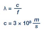
Figure 1 shows the element spacing vs. frequency, assuming there is a λ/2 antenna element spacing implementation. With these physical size constraints outlined, the RF subsystems behind the antenna can be evaluated to assess implementations required to meet the electronic channel spacing vs. frequency.

| Frequency | Element Spacing | Dual Pole I/O Spacing |
| 3 GHz | 50 mm, 2 inches | 25 mm, 1 inch |
| 10 GHz | 15 mm, 600 mils | 7.5 mm, 300 mils |
| 30 GHz | 5 mm, 200 mils | 2.5 mm, 100 mils |
Waveform Generator and Receiver Channel Spacing
Figure 2 shows an evaluation board for one of the Analog Devices transceiver products. This board contains two transceivers. Each transceiver contains two transmit and receive channels (see Figure 3) and, thus, four complete waveform generators and receivers are implemented. The board also includes a clock IC and several other I/O features for evaluation of the parts.


Although the board was not intended for the highest level of integration possible, the board provides insight into practical size limits for the waveform generator and receiver section. It is quickly apparent from the board that the transceiver product line supports every element digital antenna spacing to C-band and, with some extra effort, an X-band element spacing could be realizable.
Next, the physical size of a mating RF up/downconverter is shown in Figure 4. This particular board is intended as a test board companion for the dual transceiver board and again can be used to consider practical physical size constraints for this RF subsystem. The board is implemented with standard low cost methods, using all commercially available parts. Again, this shows that this type of implementation supports every element digital antennas up to C-band. If there is a migration to X-band, every digital element would be possible, enabling further integration with SiP (system-in-package) integration.

These two boards outline that low cost commercial implementations support every element in digital beamforming phased arrays for frequencies up to C-band. An every element implementation at X-band and beyond could be realizable with further integration or as alternative beamforming ICs can be used to reduce the number of waveform generator and receiver channels relative to the number of elements. 4:1 X-/Ku-band beamformers are now becoming commercially available and are a practical approach for low cost digital beamforming phased arrays at these frequencies.
Ka-Band Element Spacing
Next, a Ka-band antenna element spacing is considered, as shown in Figure 5. At 30 GHz the λ/2 spacing is 5 mm, which, as shown, is quite challenging for the electronics. It is practical, however, for a 4:1 analog beamformer to be implemented within this spacing directly opposite of the antenna elements. The challenge is that the physical size constraints allow little opportunity for additional components. This necessitates the need for the inclusion of LNAs or PAs within the beamforming package and for passive components, such as decoupling capacitors, to be buried within the PWB.

A fortunate design benefit for Ka-band satellite systems is that most systems separate transmit and receive functions into separate antennas. This provides the opportunity to design transmit only or receive only beamforming ICs optimized for the particular task.
Summary
The continued advancement of RF ICs for the wireless industry has become an enabler for the proliferation of digital beamforming phased array technology. It is now practical to design every element digital beamforming phased arrays with standard PWB technology for frequencies as high as C-band. At higher frequencies of X-band an every element digital implementation is practical, but extra design effort for further integration is likely required. Alternatively, a 4:1 analog beamformer could be used and offers additional space for the electronics and again allows for standard PWB implementation methods. This can become challenging at Ka-band physical size constraints. However, with integration of front-end electronics inside a beamformer package, either a subarrayed antenna architecture or an all analog beamforming system is now realizable.
About the Authors
Peter Delos is a technical lead in the Aerospace and Defense Group at Analog Devices in Greensboro, North Carolina. He received his B.S.E.E. degree from Virginia Tech in 1990 and M.S.E.E. degree from NJIT in 2004. Peter ha...


