60V/3A Step-Down DC/DC Converter Maintains High Efficiency over a Wide Range of Input Voltages
60V/3A Step-Down DC/DC Converter Maintains High Efficiency over a Wide Range of Input Voltages
by
Mark Marosek
Aug 1 2002
Introduction
The LT3430 is a monolithic step-down DC/DC converter that features a 3A peak switch current limit and the ability to operate with up to 60V input. The LT3430 runs at a fixed frequency of 200kHz and is packaged in a small thermally enhanced 16-pin TSSOP package to save space and simplify thermal management. The 5.5V to 60V input range makes the LT3430 ideal for FireWire® Peripherals (typically 8V to 40V input), as well as automotive systems requiring 12V, 24V and 42V input voltages (with the ability to survive load dump transients as high as 60V). It is designed to maintain excellent efficiencies at both high and low input-to-output voltage differentials over a wide input voltage range. Its current mode architecture adds flexible frequency compensation with no restriction on the use of a ceramic output capacitor—resulting in small solutions with extremely low output ripple voltage.
The LT3430 is pin compatible with the LT1766 (60V, 1.5A, 200kHz) and LT1956 (60V transient, 1.5A, 500kHz) step down DC/DC converters.1
LT3430 Features
- Wide input range 5.5V to 60V
- 3A peak switch current
- Small thermally enhanced 16-pin TSSOP Package
- Constant 200kHz switching frequency
- 100mΩ saturating switch
- Current mode architecture
- Peak switch current maintained over full duty cycle range
- 30µA shutdown current
- 1.2V feedback reference
- Easily synchronizable
Circuit Description
The block diagram in Figure 1 shows all of the key functions of the LT3430 step-down DC/DC converter. Its current mode architecture uses two feedback loops to control the duty cycle of the internal power switch—a transconductance error amplifier monitors the error between output voltage (via the FB pin) and an internal 1.22V reference, and a current sense comparator monitors switch current on a cycle-by-cycle basis. The LT3430 runs at a fixed frequency of 200kHz or can be externally synchronized up to 700kHz using the SYNC pin. The LT3430 includes a shutdown pin with an accurate 2.38V threshold for undervoltage lockout, and a 0.4V threshold for micropower shutdown (IQ = 30µA). The BIAS pin provides power savings by allowing control circuitry to be supplied from the output. The LT3430 also uses frequency foldback and current limit foldback to control power dissipation in the IC, external catch diode and inductor in the event of an output short circuit to ground.
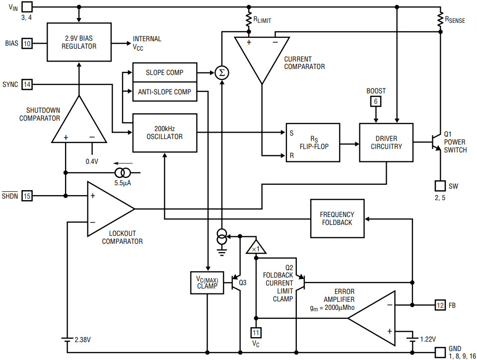
Figure 1. Simplified block diagram.
Peak Switch Current Over the Full Duty Cycle Range (Not Your Average Current Mode Converter)
The LT3430 maintains peak switch current over the full duty cycle range (wide input voltage range). Although the LT3430 uses a current mode architecture—to allow small, low noise power supply solutions—its peak switch current does not fall off at high duty cycles, unlike most current mode converters. This typical reduction of peak switch current is a result of the necessary slope compensation in the current sensing loop, which exists to prevent sub-harmonic oscillations for duty cycles above 50%. The LT3430 uses a patented process to cancel the effect of slope compensation on peak switch current without affecting frequency compensation. For applications that require high duty cycles, this offers significant advantages—including a lower inductor value, lower minimum VIN and/or higher output current capability—over typical current mode converters with similar peak switch current limits.
Efficiency
The LT3430 is designed to provide efficient solutions at both high and low input-to-output voltage differentials, over a wide input voltage range. A typical high input voltage application with a large input-to-output differential, a 42V to 5V converter, is shown in Figure 2. To obtain high efficiency at high input voltages requires fast output-switch edge rates, and minimal quiescent current drawn from the input at light loads. The BIAS pin allows power for the internal control circuitry to be supplied from the regulated output if it is greater than 3V. The peak efficiency for a 42V to 5V conversion is greater than 82% as shown in Figure 3.
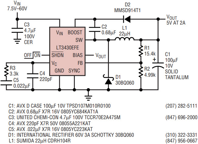
Figure 2. Efficient 42V to 5V step-down converter.
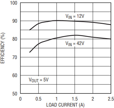
Figure 3. Efficiency of the circuit shown in Figure 2.
The LT3430 is also capable of excellent efficiencies at lower input voltages. The peak efficiency for a 12V to 5V converter is greater than 90% as is also shown in Figure 3. One important factor in achieving high efficiency for low input-to-output voltage conversions is to use a low resistance saturating switch. A prebiased capacitor, connected between the BOOST and SW pins, generates a boost voltage above the input supply during switching. Driving the switch from this boost voltage allows the 100mΩ power switch to fully saturate. Any output voltage of at least 3.3V is enough to generate the required boost supply.
Space Saving and Low Output Ripple Voltage Solutions
The high switching frequency and current mode architecture of the LT3430 combine to make it possible to design space-saving solutions with low output ripple voltage. The 200kHz switching frequency of the LT3430 reduces the inductor value required to achieve low inductor ripple current, allowing for the use of a physically smaller inductor. The current mode architecture of the LT3430 allows for flexible frequency compensation to accommodate various output voltages, load currents and output capacitor types. This flexibility allows for a small, low ESR ceramic capacitor to be used at the output—making for an extremely low output ripple voltage solution in a small space.
Figure 4 shows a 5V/2A solution for FireWire peripherals which takes advantage of the LT3430 current mode architecture by using a low ESR ceramic capacitor at the output. The circuit provides a low profile (all components less than 3.0mm height), low output ripple voltage solution. Output ripple voltage is only 26mVP–P, as shown in Figure 5, using a 22µH inductor, with VIN = 24V and VOUT = 5V at 2A.
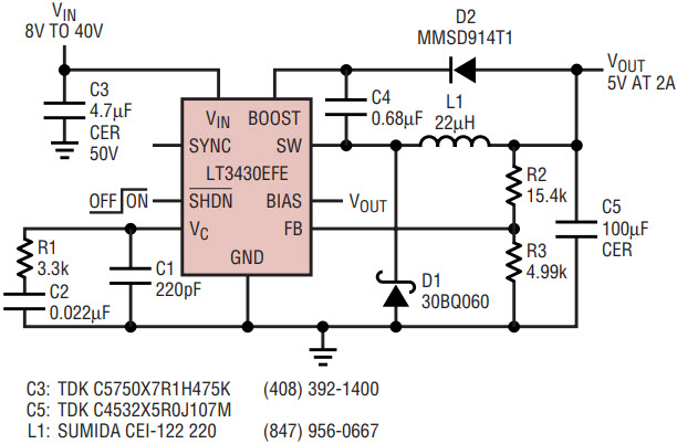
Figure 4. Low profile (max height of 3.0mm) FireWire peripheral supply with low output ripple voltage.
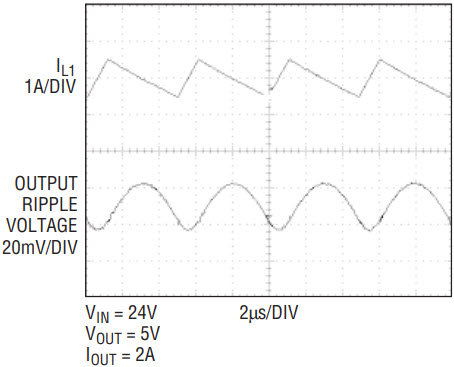
Figure 5. Output ripple voltage for the circuit shown in Figure 4.
Conclusion
The LT3430 features a 3A peak switch current limit, 100mΩ internal power switch and a 5.5V to 60V operating range, making it well suited to automotive, industrial and FireWire peripheral applications. It is highly efficient over the entire operating range, and it includes important features to save space and reduce output ripple—including a 200kHz fixed operating frequency, a current mode architecture and availability in a small thermally enhanced 16-pin TSSOP package.
Notes
1 The ‘no connect’ pins 3 and 5 of the LT1766 and LT1956 must be connected for the LT3430 to handle the increased current in the SW output (pins 2 and 5) and the VIN input (pins 3 and 4).
About the Authors
Mark Marosek is a Design Engineering Manager in Analog Devices’ Power Technology group in Milpitas, CA. His interests include monolithic Boost/Inverting/SEPIC converters and Multi-String LED drivers primarily for Automotiv...


