3ppm/°C Micropower Reference Draws Only 50µA and Operates on 2.8V
3ppm/°C Micropower Reference Draws Only 50µA and Operates on 2.8V
by
John Wright
Nov 1 1999
Introduction
The new LT1461 bandgap voltage reference is a low dropout reference that has superb temperature coefficient, tight output tolerance and low supply current. In addition, high output current together with unmeasurable thermal regulation make the LT1461 ideal for micropower precision regulator applications. To achieve these characteristics, new wafer trim techniques were developed and extensive characterization of thermal hysteresis and long-term drift were performed.
How It’s Done
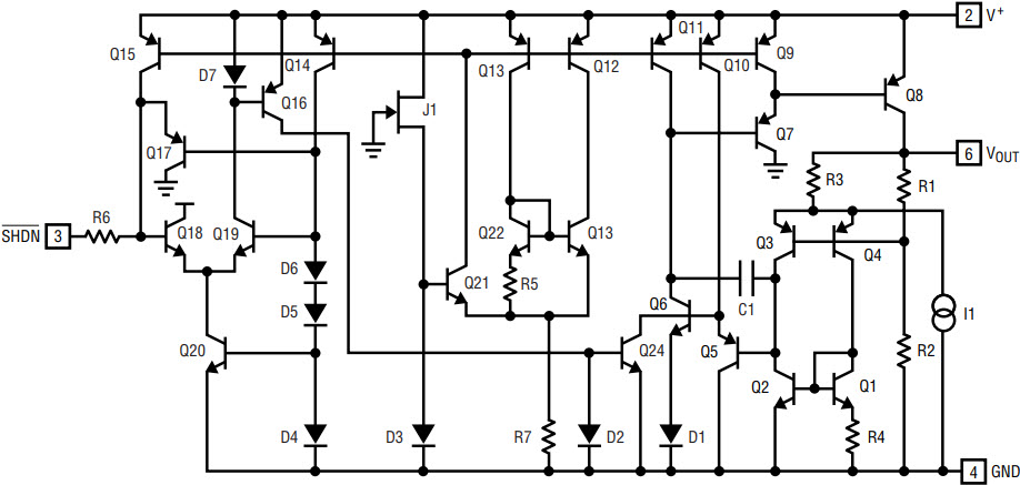
At the heart of the LT1461 is the bandgap core: Q1, Q2, Q3 and Q4 of Figure 1. Q1 and Q2 generate a ∆VBE, whereas Q3 and Q4 provide the attendant VBE. The bandgap voltage is impressed across R1, and R2 provides gain for numerous voltage options. I1 provides patented curvature compensation that modifies the ∆VBE current and greatly improves the temperature coefficient. High output current and excellent load regulation are the result of careful layout techniques and four betas of current gain from Q5 through Q8. The LT1461 has a shutdown control that can be used to turn off the reference during high output current conditions; it also has thermal shutdown or current-limit protection for the device during overload. Table 1 summarizes the performance specifications of the new reference.

Figure 1. Simplified schematic of the LT1461.
| Parameter | Conditions | Min | Typ | Max | Units |
| Output Voltage |
LT1461A | –0.04 | — | 0.04 | % |
| LT1461B | –0.06 | — | 0.06 | ||
| LT1461C | –0.08 | — | 0.08 | ||
| LT1461D | –0.15 | — | 0.15 | ||
| Output Voltage Temperature Coefficient |
LT1461A | — | — |
3 | ppm/°C |
| LT1461B | — | — | 7 | ||
| LT1461C | — | — | 12 | ||
| LT1461D –40°C to 125°C | — | — | 20 | ||
| Load Regulation | Sourcing 0mA to 50mA | — | 12 | 30 | ppm/mA |
| Dropout Voltage | Sourcing 1mA | — | 0.13 | 0.3 | V |
| Supply Current | No Load | — | 35 | 50 | µA |
| Output Voltage Noise | 0.1Hz ≤ f ≤ 10Hz | — | 8 | — | ppmp-p |
| Long-Term Drift of Output Voltage | — | — | 60 | — | ppm/√kHr |
| Thermal Hysteresis | –40°C to 85°C | — | 65 | — | ppm |
How It’s Really Done
In order for the factory to trim the output voltage to a very tight tolerance, four pins of the package are dedicated to trimming R1. This trim allows the LT1461 output voltage to be adjusted to better than 0.02%. The final specification, however, is a conservative 0.04%, because the part is measured with different factory testers and a safety margin or guardband is applied for thermal hysteresis.
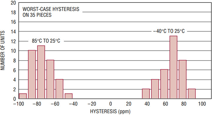
The idea of this guardband is to ensure that the parts will remain 0.04% accurate even after they are exposed to temperature excursions of –40°C to 85°C. When a part is trimmed to high accuracy, its output voltage is valid only for the mechanical stress conditions that are present at the time of trim. The amount of stress will change with temperature because the thermal coefficient of expansion is different between the plastic package and the silicon chip. When the part returns to its “trimmed” temperature, there is no guarantee that the stress returns to exactly the initial amount, and the output voltage will be slightly different. This difference is called “thermally induced hysteresis shift” or “thermal hysteresis” and is expressed in parts per million (ppm). Figure 2 shows a distribution plot of thermally induced hysteresis shift on parts that were cycled several times between –40°C and 85°C. The LT1461 initial accuracy is specified broadly enough to include this hysteresis shift.

Figure 2. –40°C to 85°C hysteresis.
The output trim on the LT1461 uses all available pins on the package, so the temperature coefficient must be trimmed at wafer sort. If a reference has its bandgap voltage trimmed to the proper target or “bogie,” it will have a near zero temperature drift. The problem is that the bogie moves with process variations and can differ from die to die. The solution is to measure the temperature coefficient at wafer sort and use an algorithm to correct the bandgap voltage. This requires wafer sorts at 75°C and 25°C to establish the drift. For example, if the bandgap voltage is trimmed to 1.2000V at 75°C and it moves 300µV to 1.2003V at 25°C, this corresponds to a –5ppm/°C drift. Once the TC is known, the bandgap voltage can easily be trimmed for zero TC by adjusting R3. The TC distribution widens when the parts are assembled in plastic because of stress on Q3 and Q4.
What the User Knows
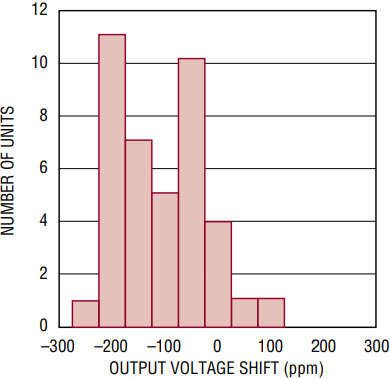
Users encounter several problems when applying precision references and again thermal hysteresis is front and center. When a reference is soldered into a PC board, the elevated temperature and subsequent cooling cause stress that is very different from stress that is caused by automatic testers at the LTC factory. Additionally, there is now an unrelieved mechanical bias on the leadframe when the solder cools. Figure 3 shows the SO-8 LT1461 output shift of about –100ppm after IR soldering onto a PC board. After 336 hours, as the stress relaxes, the output voltage typically shifts about 45ppm back toward the initial state where the device was factory trimmed.

Figure 3. Typical distribution of output voltage shift after soldering onto PC board.
Another type of stress is caused if a PC board is flexed, for example when held in a card cage. The stress on the board is transmitted directly to the IC package. A simply way to reduce the stress-related shifts is to mount the reference near the short edge of the PC board or in a corner. The board edge acts as a stress boundary, or a region where the flexure of the board is minimum. The package should be mounted so that the leads absorb the stress and not the package. (See “Understanding and Applying Voltage References,” in Linear Technology VII:2 and VII:3, June and August, 1997, for more information on the effects of stress on voltage reference performance and techniques for mitigating it.)
Long-Term Drift
Some manufactures are now touting phenomenal long-term drift specifications. Long-term drift cannot be extrapolated from accelerated high temperature testing. This erroneous technique gives drift numbers that are wildly optimistic. The only way long-term drift can be measured is over the time interval of interest. The erroneous technique uses the Arrhenius Equation to derive an acceleration factor from elevated temperature readings. The equation is:

where: EA = Activation Energy (assume 0.7)
K = Boltzmann’s Constant
T2 = Test Condition Temperature in Kelvin
T1 = Use Condition Temperature in Kelvin
To show how absurd this technique is, compare the LT1461 data. Typical 1000hr long-term drift at 30°C = 60ppm. The typical 1000hr longterm drift at 130°C = 120ppm. From the Arrhenius Equation the acceleration factor is:

The erroneous projected long-term drift is:

For a 2.5V reference, this corresponds to a 0.39µV shift after 1000 hr. This is pretty hard to determine (read impossible) if the peak-to-peak output noise is larger than this number. As a practical matter the best laboratory reference available has long-term drift of 1.5µV/mo. This performance is only available from the very best subsurface Zener references using specialized heating techniques.
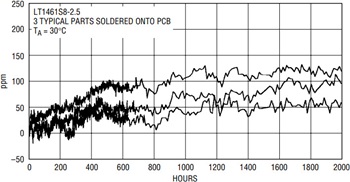
The LT1461 long-term drift data was taken with parts that were soldered onto PC boards as in a “real world” application. The boards were then placed in a constant-temperature oven with TA = 30°C and their outputs were scanned regularly and measured with an 8.5 digit DVM. Figure 4 shows the long-term drift of three typical LT1461S8-2.5s soldered into a PC board. This is the best performance we have measured on an IC voltage reference that is not based on a subsurface Zener.

Figure 4. Long-term drift.
Conclusion
The LT1461 series reference meets the growing need for low power, high accuracy and low temperature coefficient, while simultaneously serving micropower precision regulator applications. This new bandgap reference comes in the 8-lead SO package. It is available in 2.5V and will be available in 4.096V, 5.0V and 10V options.


