16-Bit Parallel DAC Has 1LSB Linearity, Ultralow Glitch and Accurate 4-Quadrant Resistors
16-Bit Parallel DAC Has 1LSB Linearity, Ultralow Glitch and Accurate 4-Quadrant Resistors
Feb 1 1999
Today’s fast paced marketplace has developed a major appetite for high resolution, high accuracy, fast digital-to-analog converters. System requirements in instrumentation, automatic test equipment, communications, waveform generation, data acquisition and feedback control systems, among many other applications, have fueled the need for 16-bit digital-to-analog converters. Not only does the converter need to meet the stringent speed and accuracy requirements of the system, it needs to do so in both unipolar (0V to 10V) and bipolar (±10V) modes of operation without degradation. To meet and exceed these requirements, Linear Technology introduces its LTC1597 16-bit parallel, current output, low glitch, multiplying DAC with 4-quadrant resistors. Key features of the new DAC include:
- ±1LSB maximum INL and DNL over the industrial temperature range.
- On-chip 4-quadrant resistors allow precise 0V to 10V, 0V to –10V or ±10V outputs.
- Ultralow, < 1nV-s midscale glitch impulse.
- Small 28-pin SSOP package.
- Low supply power consumption: 10µW typical.
- Pin-compatible with the LTC1591 14-bit parallel, current output, low glitch, multiplying DAC with 4-quadrant resistors.
Unique Features of the LTC1597
The LTC1597 operates from a single 5V supply and provides both unipolar 0V to –10V or 0V to 10V and bipolar ±10V output ranges from a 10V or –10V reference input using a single or dual external op amp. The device achieves bipolar operation using three additional on-chip precision resistors. The DAC consists of a precision thin-film R/2R ladder for the thirteen LSBs. The three MSBs are decoded into seven segments of resistor value R, as shown in Figure 1. R is nominally 48k. Each of these segments and the R/2R ladder carry an equally weighted current of one-eight of full-scale. The feedback resistor, RFB, and 4-quad- rant resistor, ROFS, have a value of R/4. 4-quadrant resistors R1 and R2 have a magnitude of R/4.
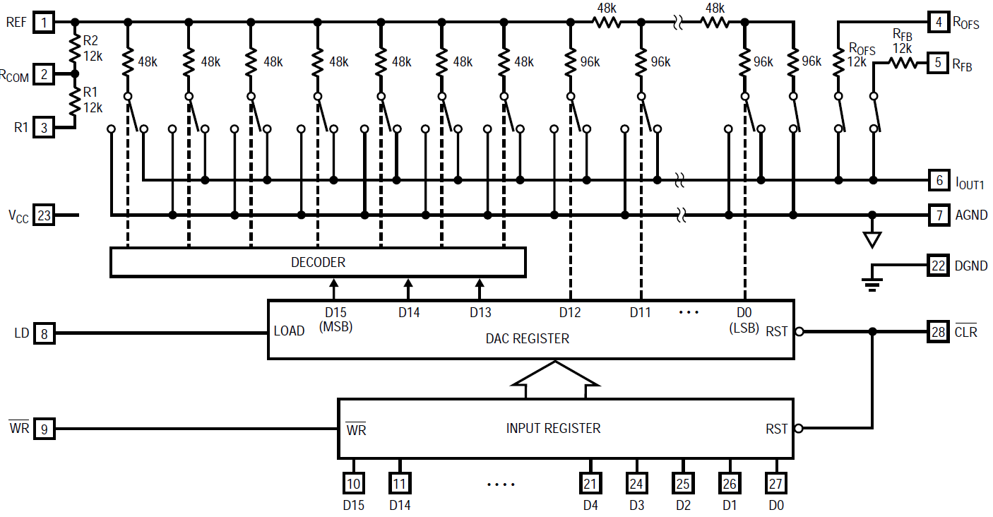
Figure 1. The LTC1597 16-bit CMOS DAC uses a precision thin-film modified R/2R architecture to provide unsurpassed accuracy and stability. Accurate 4-quadrant multiplication applications are now possible with on-chip resistors R1, R2 and ROFS. A built-in deglitcher reduces glitch impulse to 1nV-s.
The reference pin presents a constant input impedance of R/8 in unipolar mode and R/12 in bipolar mode. The output impedance of the current out- put pin, IOUT1, varies with DAC code.
An added feature of the LTC1597 is a proprietary deglitcher that reduces the glitch energy to below 1nV-s over the DAC’s output voltage range.
The LTC1597 has a 16-bit parallel input data bus and is double buffered with two 16-bit registers. The double buffered feature permits the updating of several DACs simultaneously. The WR signal updates the input register and the LD signal loads the DAC register. The deglitcher is activated on the rising edge of the LD signal.
The versatility of the interface also allows the use of the input and DAC registers in a master/slave or edge-triggered configuration. This mode of operation occurs when WR and LD are tied together to act as a clock signal.
The asynchronous clear pin (CLR) resets the LTC1597 to zero scale and the LTC1597-1 to midscale. CLR resets both the input and DAC registers. The LTC1597 also features a power-on reset.
16-Bit Accuracy Over Temperature
The LTC1597 has ultralow linearity drift of well below ±0.2LSB from –45°C to 85°C. This allows the LTC1597 to hold its accuracy of 1LSB integral nonlinearity (INL) and differential nonlinearity (DNL) over time and temperature. In the past, the only DACs that approached this accuracy over temperature were of the autocalibrated type. These DACs were very large, very expensive and therefore not very practical for most applications.
Figures 2a and 2b show the typical INL and DNL curves of the LTC1597. The outstanding 0.25LSB INL, 0.15 LSB DNL (typical) and very low drift allow a maximum 1LSB specification over the extended industrial temperature range. For optimum performance, the REF pin of the LTC1597 should be driven by a source impedance of less than 1kΩ. However, the DAC has been designed to minimize source impedance effects. An 8kΩ source impedance degrades both INL and DNL by a mere 0.2LSB.
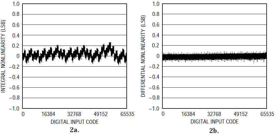
Figure 2. The outstanding INL and DNL (typically less than 0.25LSB) and very low linearity drift allow a maximum 1LSB spec to be guaranteed over the industrial temperature range.
Fast Settling: Less than 2µs to within 0.0015% of Full-Scale
Now system designers no longer have to make tough decisions in the trade-off between accuracy and speed. The solution is here. The combination of the LTC1597 DAC and the LT1468 op amp provides an industry first: superb 16-bit settling of less than 2µs for a 10V step while maintaining 1LSB DC accuracy.
Figure 3 shows the application circuit for unipolar mode. Figure 4 shows the resulting full-scale 10V step settling time of the LTC1597/LT1468 combination. With a 20pF feedback capacitor, the optimized settling time to 0.0015% is an amazing ≈1.7µs. A detailed discussion of 16-bit settling time can be found in Linear Technology Application Note 74, “Component and Measurement Advances Ensure 16-Bit DAC Settling Time.”
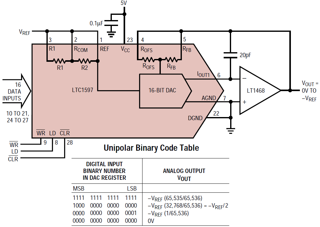
Figure 3. With a single external op amp, the LTC1597 performs 2-quadrant multiplication with ±10V input and 0V to –VREF output. With a fixed –10V reference, it provides a precision 0V to 10V unipolar output.
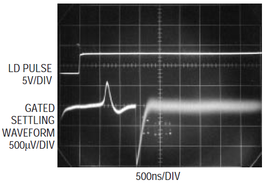
Figure 4. When used with the LT1468 and a 20pF feedback capacitor (see Figure 3), the LTC1597 can settle in an amazing 1.7µs to within 0.0015%. The top trace shows the LD pulse; the bottom trace shows the gated settling waveform settling to 1LSB in 1.7µs.
The ability to minimize settling time is limited by the need to null the DAC output capacitance, which varies from 70pF to 115pF, depending on code. This capacitance at the amplifier input combines with the feedback resistor to form a zero in the closed-loop frequency response in the vicinity of 200kHz–400kHz. Without a feedback capacitor, the circuit will oscillate. The choice of 20pF stabilizes the circuit by adding a pole at 1.3MHz to limit the frequency peaking and also optimizes settling time. The settling time to 16-bit accuracy is theoretically bounded by 11.1 time constants set by the feedback resistance and capacitance.
Ultralow 1nV-s Glitch
Glitches in a DAC’s output when it updates can be a big problem in precision applications. Usually, the worst-case glitch occurs when the DAC output crosses midscale. The LTC1597’s new proprietary deglitcher reduces the output glitch impulse to 1nV-s, which is at least ten times lower than any of the competition’s 16-bit voltage output DACs. In addition, the deglitcher makes the glitch impulse uniform for any code. Figure 5 shows the output glitch for a mid-scale transition with a 0V to 10V output range.
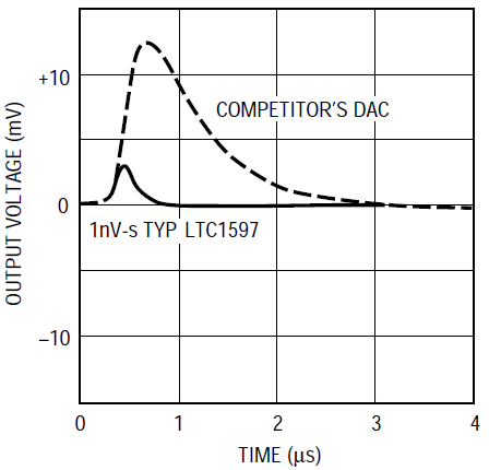
Figure 5. The proprietary deglitcher reduces 0000 the output glitch to less than 1nV-s, which is ten times less than any other 16-bit, voltageoutput DAC. Further, the deglitcher makes the glitch uniform, independent of code.
Unipolar 0V to 10V Outputs with a Single Op Amp
Figure 3 shows the circuit for a 0V to 10V output range. The DAC uses an external reference and a single op amp in this configuration. This circuit can also perform 2-quadrant multiplication where the REF pin is driven by a ±10V AC input signal and VOUT swings from 0V to –VREF.
Bipolar ±10V Output with Two Op Amps
The LTC1597 contains all the 4-quadrant resistors necessary for bipolar operation. For a fixed 10V reference, the circuit shown in Figure 7 gives a precision –10V to 10V output swing, with a minimum of external components: a feedback capacitor and a dual op amp. The bipolar zero error is 8LSB maximum over temperature. If two LT1468 op amps are used instead of the LT1112, the circuit can perform wider bandwidth 4-quadrant multiplication, where the reference input is driven by a ±10V AC input signal and VOUT swings ±10V.
Figure 6 shows a graph of the multiplying mode total harmonic distortion and noise of the LTC1597/LT1468 combination in both unipolar and bipolar modes of operation. For AC signals less than 40kHz, the THD+noise is superb (better than 90dB) and is still very good out to 100kHz (78dB). Filtering at the output of the LT1468 is necessary to reduce the noise bandwidth to acceptable levels. The wider the bandwidth, the higher the noise floor.
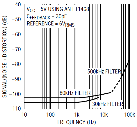
Figure 6a. Unipolar-mode full-scale: the noise and distortion (N + D) is less than –96dB for signal frequencies up to 30kHz. Out to 100kHz, the N + D is less than –78dB.
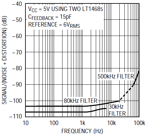
Figure 6b. Bipolar-mode zero-scale: the N + D is less than –96dB for signal frequencies up to 30kHz. Out to 100kHz, the N + D is less than –82dB.
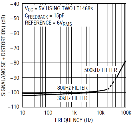
Figure 6c. Bipolar-mode full-scale: the (N + D) is less than –96dB for signal frequencies up to 30kHz. Out to 100kHz, the N + D is less than –79dB.
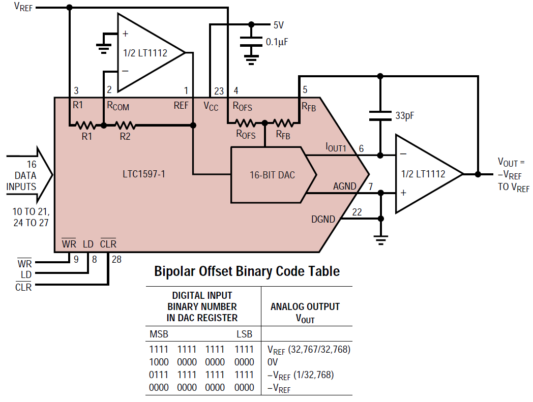
Figure 7. With a dual op amp, the LTC1597 performs 4-quadrant multiplication. With a fixed 10V reference, it provides a ±10V bipolar output. For fast bipolar settling applications, an LT1468 can be used for the output amplifier.
17-Bit Sign Magnitude DAC Gives Perfect Bipolar Zero
Figure 8 shows a novel application of the LTC1597, a 17-bit sign magnitude DAC, and the resulting output coding. This circuit has an extremely accurate bipolar zero error, which is the offset voltage of the current-to-voltage op amp plus the bias current times the DAC feedback resistor. For the LT1468, this corresponds to a maximum bipolar zero error of 0.92LSB (140µV) at 17 bits for room temperature. The circuit uses the LTC1597 in its unipolar mode with the reference input inverted (–VREF, by means of R1 and R2 and an external op amp) for the output voltage range 0V to VREF. When the sign bit changes, the analog switch changes the reference input polarity to noninverting (VREF) for the output range 0V to –VREF.
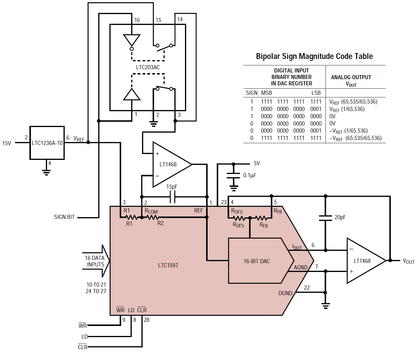
Figure 8. This 17-bit sign-magnitude DAC uses the LTC1597 in its unipolar mode with the reference bit inverted (–VREF) for the output range 0V to VREF. When the sign bit changes, the analog switch changes the reference input polarity to noninverting (VREF) for the output range 0V to –VREF. The resulting circuit produces an impressive bipolar zero error of 140µV (0.92LSB) max at room temperature—less than 1LSB at 17 bits.
94dB SFDR Digital Sine Wave Generator
Figure 9 shows the circuit diagram for a variable frequency digital waveform generator. The circuit shows the bipolar configuration for the LTC1597 but the unipolar configuration will work just as well. For a sampling frequency of 50kHz and an output sine wave frequency of 1kHz, the second harmonic distortion is –94dB and the third harmonic is –101dB. The on-chip deglitcher circuit minimizes the code-dependent glitch (which causes distortion) by making the glitch impulse both ultralow and uniform with code.
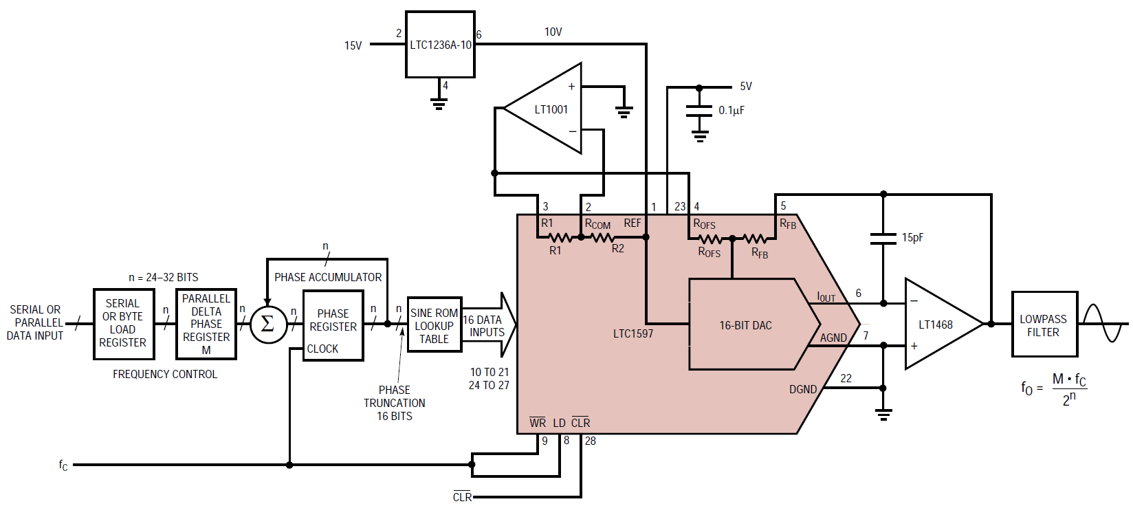
Figure 9. This digital waveform generator produces a 1kHz sine wave with a second harmonic distortion of –94dB. The sampling frequency is 50kHz.
Op Amp Selection Considerations
A significant advantage of the LTC1597 is the ability to choose the I-to-V output op amp to optimize system accuracy, speed, power and cost. Table 1 shows a sampling of op amps and their relevant specifications for this application.
| Amplifier Specifications |
||||||||
| Amplifier | VOS µV | IB nA | AOL V/mV | Voltage Noise nV/√Hz | Current Noise pA/√Hz | Slew Rate V/µs | Gain Bandwidth Product MHz | Power Dissipation mW |
| LT1001 | 25 | 2 | 800 | 10 | 0.12 | 0.25 | 0.8 | 46 |
| LT1097 | 50 | 0.35 | 1000 | 14 | 0.008 | 0.2 | 0.7 | 11 |
| LT1112 (dual) | 60 | 0.25 | 1500 | 14 | 0.008 | 0.16 | 0.75 | 10.5/op amp |
| LT1124 (dual) | 70 | 20 | 4000 | 2.7 | 0.3 | 4.5 | 12.5 | 69/op amp |
| LT1468 | 75 | 10 | 5000 | 5 | 0.6 | 22 | 90 | 117 |
The LTC1597 is designed to minimize the sensitivity of INL and DNL to op amp offset; this sensitivity has been greatly reduced compared to that of competing multiplying DACs. Figure 10 summarizes the effects of op amp offset for both modes of operation. Note that the bipolar LSB size is twice its unipolar counterpart. As Figure 10 shows, op amp offset has a minimal effect on DAC linearity; it merely shifts the end points.
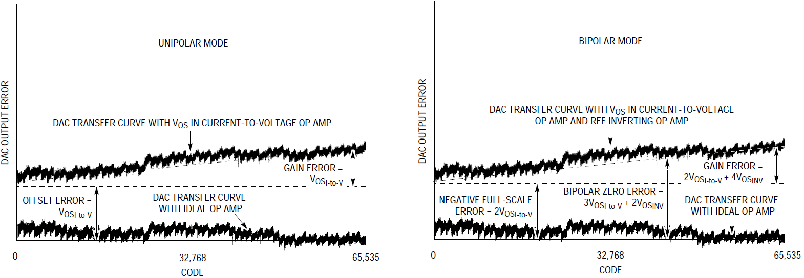
Figure 10. The effect of op amp offset on the LTC1597 gain and offset errors in unipolar mode (left) and bipolar mode (right); op amp offset has virtually no effect on DAC linearity; it merely shifts the end points.
The amplifier’s input bias current, which flows through the feedback resistor, adds to the output offset voltage. The amplifier’s finite DC open-loop gain also degrades accuracy. The DAC gain error is inversely proportional to the open-loop gain and feedback factor of the op amp. In unipolar mode at full-scale the feed-back factor is 0.5; for a 0.2LSB of gain error (REF = 10V) at 16 bits, the open- loop amplifier gain should be greater than 650,000.
The op amp’s input voltage and current noise also limit DC accuracy. Noise effects accuracy similarly to voltage and current offsets and adds in an RMS fashion. As with any precision application, and with wide bandwidth amplifiers in particular, the noise bandwidth should be minimized with a filter on the output of the op amp to maximize resolution.
Referring to Table 1, the LT1001 provides excellent DC precision, low noise and low power dissipation. The LT1468 provides the optimum solution for applications requiring DC precision, low noise and fast 16-bit settling.
Conclusion:
Wherever system requirements demand true 16-bit accuracy over temperature, the LTC1597 provides the best solution. The LTC1597 has outstanding 1LSB linearity over temperature, ultralow glitch impulse, on-chip 4-quadrant resistors, low power consumption, asynchronous clear and a versatile parallel interface. Combined with the LT1468 op amp, the LTC1597 provides the best in its class, 1.7ms settling time to 0.0015%, while maintaining superb DC linearity specifications.
About the Authors


