EM-Plugs
Overview
Features and Benefits
EM-Plug models are an EM-based RF digital twin capturing RF IC behavior across substrates, layouts and transitions for high-frequency designs. They’re lightweight, modular, and have accurate EM-level modeling.

- Why it matters: Matching and bandwidth change with substrate and layout, but these effects cannot be captured using S-parameters alone.
- The blind spot: S-parameters place the reference plane at the chip boundary or 50Ω trace, leaving substrate- and transition-dependent behavior behind the reference plane.
- What changes: EM-Plug models bring transition behavior into simulation, eliminating the need for a “trial and error”-based test PCB approach.
- CAD tool support: EM-Plug models are provided for ANSYS HFSS. Models are not encrypted, enabling import into other 3D EM solvers as needed.
The compatible parts listed was last updated on 5/7/2026.
Compatible Parts
- ADTR1101
- ADTR1104
- ADPA7008
- ADPA7006
- ADPA7005
- ADPA1112
- ADPA1106
- ADL8106
- ADL8102
- ADL8108
- ADRF5740
- ADRF5720
- ADRF5721
- ADRF5730
- ADRF5731
- ADRF5476
- ADRF5700
- ADRF5714
- ADRF5715
- ADRF5716
- ADRF5717
- ADRF5030
- ADRF5031
- ADRF5044
- ADRF5045
- ADRF5048
- ADRF5049
- ADRF5420
- ADRF5440
- ADRF5026
- ADRF5027
- ADRF5424
- ADRF5050
- ADRF5051
- ADRF5080
- ADRF5022
- ADRF5023
- ADRF5020
- ADRF5021
- HMC797APM5E
- HMC994APM5E
What Are EM-Plugs and How Do They Work?
EM-Plug models separate the intrinsic RF core from the EM-modeled interface at the on-chip reference plane. Together, 3D EM simulation of the EM-Plug model and the RF core represent the complete behavior in the layout.
- RF core: Intrinsic/core RF IC behavior.
- EM-Plug: Interface EM model of the chip to substrate including the transition(layout).
- Combined model: Input EM-Plug + RF core + EM-Plug = Complete RF behavior.

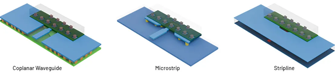
Package and transition examples across multiple integration styles.
What EM-Plug Models Enable
- No PCB trial-and-error: Matching and transition optimization without building test boards or fixtures, enabling higher first-pass success.
- Lightweight, practical simulation: Much faster (hours to minutes) and easier to iterate than full-chip encrypted EM models.
EM Plug

- Chip to PCB transition
- Simulation & measurement based
- Fast overall design time
- No IP restriction
- Tool independent
- Heavy computation not required
Full Wave EM Model

- Complete chip and PCB transition
- Simulation based
- Long simulation time
- Requires encryption, involves IP
- Tool independent due to encryption
- Heavy computation required
Matrix Board

- Blind PCB transitions
- Measurement based
- Manufacturing time
- No IP restriction
- Requires PCB tool expertise
- Manufacturing cost
EM-Plug model vs. full-wave EM model vs matrix board (workflow comparison).
- Modular design exploration: Multiple transitions and PCB stack-ups could be analyzed.
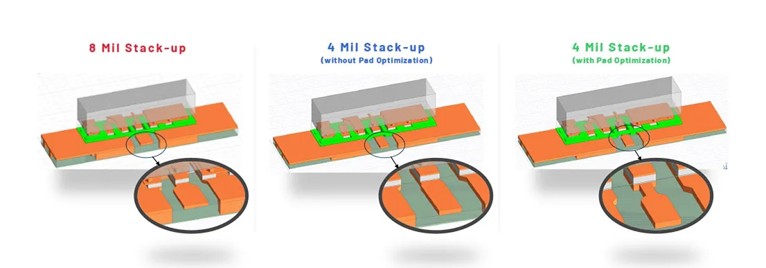
- Capture all critical variables: Landing pattern, stack-up (thickness/εr), coplanar/microstrip/stripline, solder/mask, and placement/bondwire.
Use EM sweeps to evaluate implementation sensitivity and optimize early.
Documentation & Resources
-
EM-Plugs for RF ICs : Practical EM Models for Fast and Accurate RF Design4/19/2026PDFundefined