
Overview
Design Resources
Description
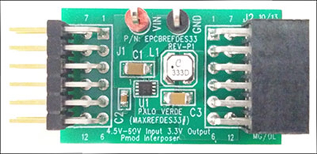
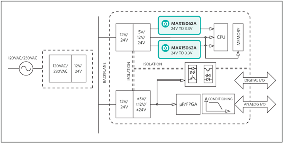
The Palo Verde MAXREFDES33 subsystem reference design (Figure 1) demonstrates the application of the MAX15062A 60V, 300mA ultra-small, high-efficiency, synchronous step-down converter. The reference design operates over a wide 4.5V to 60V input voltage range, and provides up to 300mA at 3.3V output. The device features undervoltage lockout, overcurrent protection, and thermal shutdown. The MAX15062A switches at a fixed frequency of 500kHz, and delivers a peak efficiency of 86.77% with the supplied components when the input is 24V. This general-purpose power solution can be used in many different types of power applications, such as 4–20mA current loops, HVAC and building control, high-voltage LDO replacement, general-purpose point-of-load, etc. In this reference design, the MAX15062 performs in 24V input applications, such as industrial sensors, process control, etc.
Features & Benefits
Applications
- Industrial sensors
- Process control
- 4–20mA current loops
- General-purpose point-of-load
- High-voltage LDO replacement
- HVAC and building control
- PLCs
Features
- Minimal external components and low system cost
- Versatile functionality allows stocking of fewer DC-DC regulators
- Low power dissipation
- Reliable operation in adverse industrial environments
- Pmod™-compatible form factor
Parts Used
Details Section
The Palo Verde subsystem reference design is a high-efficiency, high-voltage, synchronous step-down DC-DC converter solution with integrated MOSFETs. Palo Verde operates over a wide 4.5V to 60V input voltage range. The converter delivers output current up to 300mA at 3.3V. When EN/UVLO and VCC UVLO are satisfied, an internal power-up sequence soft-starts the error-amplifier reference, resulting in a clean monotonic output-voltage soft-start independent of the load current. The VOUT pin monitors the output voltage through an internal resistor-divider. RESET transitions to a high-impedance state 2ms after the output voltage reaches 95% of regulation. The device selects either PFM or forced-PWM mode depending on the state of the MODE pin at power-up (this reference design sets the device in PWM mode). By pulling the EN/UVLO pin to low, the device enters the shutdown mode and consumes only 2.2µA (typical) of standby current.
The reference design switches at a fixed frequency of 500kHz, and delivers a peak efficiency of 86.77% with the supplied components when the input is 24V.
This reference board is designed in a Pmod-compatible form factor with IO pass-through, but can be used in any 4.5V–60V to 3.3V power application up to 300mA.
Required Equipment:
- Palo Verde (MAXREFDES33) board
- One 24V, 1A minimum power supply that shows the output current
- One electronic load
- One voltmeter
- Turn off the power supply.
- Connect the positive terminal of the power supply to the VIN connector of the MAXREFDES33 board.
- Connect the negative terminal of the power supply to the GND connector of the MAXREFDES33 board.
- Connect the positive terminal of the electronic load to J2-6 of the MAXREFDES33 board.
- Connect the negative terminal of the electronic load to J2-5 of the MAXREFDES33 board.
- Connect the positive terminal of the voltmeter to the positive terminal of the electronic load.
- Connect the negative terminal of the voltmeter to the negative terminal of the electronic load.
- Turn on the power supply.
- Set the electronic load to a constant current between 0 to 300mA.
- Verify the voltmeter reading is 3.3V ±0.05V.
The Palo Verde design was tested using a 24V input voltage. The performance under other input conditions can be captured with a similar setup. Refer to the MAX15062 data sheet for detailed performances in other application conditions.
The power efficiency vs load current is illustrated in Figure 2.

Figure 2. Power efficiency vs. current load for 24V input
Figure 3 and Figure 4 display the ripple at no load (ripple is 6mV peak-peak) and 300mA load (ripple is 8mV peak-peak), respectively. Channel 1 in the oscilloscope screen shot is voltage at the LX pin. Channel 2 in the oscilloscope screen shot is voltage at the VOUT pin.

Figure 3. Output ripple at 0mA load

Figure 4. Output ripple at 300mA load
Figure 5 displays the load transient response when the load is stepped from 5mA to 150mA, and then dropped back to 5mA again.The transient voltage is about 60mV.

Figure 5. Transient response when load steps from 5mA to 150mA
Figure 6 displays the load transient response when the load is stepped from 150mA to 300mA, and then dropped back to 150mA again.The transient voltage is also about 60mV.

Figure 6. Transient response when load steps from 150mA to 300mA.
Documentation & Resources
-
MAXREFDES33 Design Files4/1/2021ZIP446 K
Support & Training
Search our knowledge base for answers to your technical questions. Our dedicated team of Applications Engineers are also available to answer your technical questions.