


Overview
Design Resources
Description
The MAXREFDES1274 is a buck converter using the MAX17501F high-efficiency, high-voltage, synchronous step-down DC-DC converter with integrated MOSFETs and internal compensation. This design produces a 5V output at up to 500mA from a wide input range of 6.5V to 60V. The device features peak-current-mode control with pulse-width modulation (PWM). The MAXREFDES1274 was optimized for small solution size and is laid out on a two-layer PC board.
Features & Benefits
- Ultra-Compact Layout (31.52mm2 Footprint Size)
- Wide Input Voltage Range of 6.5V to 60V
- 500mA Output Current
- 5V Output Voltage
- 600kHz Switching Frequency
- Adjustable Soft-Start Time (SS)
- Enable/Undervoltage Lockout (EN/UVLO)
- Open-Drain Reset Output Functionality
- Peak-Current-Mode Control with Pulse-Width Modulation (PWM)
Parts Used
Details Section
The MAXREFDES1274 is a buck converter using the MAX17501F high-efficiency, high-voltage, synchronous step-down DC-DC converter with integrated MOSFETs and internal compensation. This design produces a 5V output at up to 500mA from a wide input range of 6.5V to 60V. The device features peak-current-mode control with pulse-width modulation (PWM). The MAXREFDES1274 was optimized for small solution size and is laid out on a two-layer PC board.
Its other features include the following:
- Ultra-Compact Layout (31.52mm2 Footprint Size)
- Wide Input Voltage Range of 6.5V to 60V
- 500mA Output Current
- 5V Output Voltage
- 600kHz Switching Frequency
- Adjustable Soft-Start Time (SS)
- Enable/Undervoltage Lockout (EN/UVLO)
- Open-Drain Reset Output Functionality
- Peak-Current-Mode Control with Pulse-Width Modulation (PWM)
This document demonstrates the MAX17501F for a 5V application, allowing for a load up to 500mA at 5V. This design was optimized for a small solution size to demonstrate that competitive efficiency is achievable with small components on a two-layer PCB. Table 1 is an overview of the design specifications.
| PARAMETER | SYMBOL | MIN | TYP | MAX |
| Input Voltage | VIN | 6.5V | 24V | 60V |
| Output Voltage | VOUT | 5V | ||
| Output Current | IOUT | 500mA | ||
| Output Power | POUT | 2.5W | ||
| Peak Efficiency | η | 94.8% | ||
| Output Ripple | ΔVOUT | < 12mV | ||
| Output Undershoot | VUS | < 20mV | ||
| Output Overshoot | VOS | < 20mV | ||
| Frequency | fSW | 600kHz | ||
| Footprint Size* | 31.52mm2 | |||
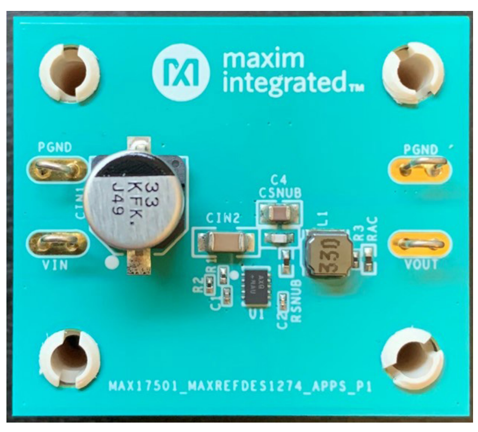
This document describes the hardware in Figure 1. It provides a systematic technical guide to design a stepdown converter using the MAX17501F, a fixed 5V output, high-efficiency, high-voltage, synchronous step-down DC-DC converter with integrated MOSFETs. The power supply was built and tested. The details follow later in this document.
DC-DC buck converters are commonly used for their optimal output efficiency, low heat dissipation, high accuracy, small transient response, and low cost. There are two types of step-down DC-DC converters: synchronous and asynchronous buck converters.
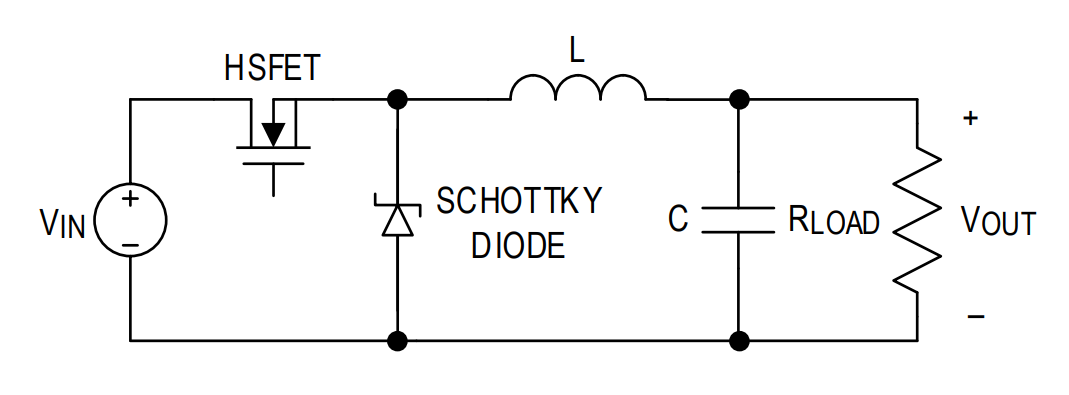
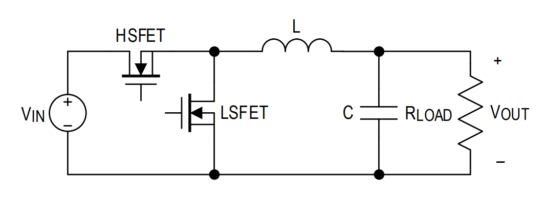
Synchronous buck converters are widely used today in compact designs because of the superior efficiency to the asynchronous buck converter. The asynchronous buck topology uses an external Schottky diode for the low-side switch (Figure 2a) while the synchronous buck topology integrates a low-side MOSFET (LSFET) (Figure 2b). This reduces power loss and increases power efficiency significantly because it eliminates the diode's IF x VF power loss in exchange for the power lost across the MOSFET's low on-resistance.
Power dissipation across the diode in the asynchronous solution:
Power dissipation across the MOSFET in a synchronous solution:
Design Procedure for Synchronous Buck Converter Using MAX17501
The design procedure provides a step-by-step process for power supply designers to select external components. The component designators in this document are in reference to the MAXREFDES1274 schematic. All other terms and variables are from the MAX17501 data sheet.
No feedback components are needed because this design uses the MAX17501F, a preset 5V output version of the MAX17501. The FB/VO pin should be connected to the VOUT. Instead of connecting directly to VOUT, this design connects to a 40Ω resistor between the FB/VO and VOUT, named RAC. This component is included for the ease of testing to obtain a loop response bode plot. RAC is not included in the total solution size because is not essential to the operation.
Step 1. Base Design
The initial design was produced by the EE-Sim®, an online design and simulation environment, which greatly streamlines the design of switch-mode DC-DC converters. The EE-Sim® design and simulation environment considers input voltage range, ripple specifications, output voltage, output current, and design priorities. Once the EE-Sim® design and simulation environment produced a schematic, the components were later tweaked to improve performance and minimize solution size. The EE-Sim® produced the following component values, which are later tweaked for the end design:
L = 47µH
CIN = 1µF
COUT = 3 x 10µF
Step 2. Inductor
Small size is the top priority of this design. So, the inductor was selected as the first component as it is typically the largest component in a power supply design. Three key inductor parameters must be specified for operation with the device: inductance value (L), inductor saturation current (ISAT), and DC resistance (RDCR).
The MAX17501 data sheet recommends to select the inductor with the following equation:
The minimum inductor size for CCM is:
where di is assumed to be 15% of the full load (500mA x 15% = 75mA).
A value of 33µH was selected as small footprint inductors of this value are readily available.
The ASPI-4030S-330M was selected as a 33µH inductor with a saturation current of 1.1A, well above the output current for this design. A low 330mΩ DCR minimizes losses in the inductor.
| PARAMETER | VALUE |
| Inductance | 33μH |
| Footprint Size | 4mm x 4mm |
| DC Resistance | 330mΩ |
| Current Rating | 0.84A |
| Saturation Current | 1.1A |
Step 3. Output Capacitor
The MAX17501 data recommends to connect a minimum of 10µF (1206) capacitor at the output for fixed 3.3V and 5V output voltage versions.
A single ceramic output capacitor is used for this deign to minimize solution size although the EE-Sim® generated schematic recommends three 10µF in parallel. This single capacitor must have a derated value of at least 10µF at 5V DC.
The GRM21BD71A226ME44, a 22µF ceramic capacitor with a 5V derating of ~47% of the nominal capacitance (approximately 10.34µF), was selected. Temperature stability was sacrificed for the small solution size.
| PARAMETER | VALUE |
| Nominal Capacitance | 22μF |
| 5V Derated Capacitance | Approx. 10.34µF |
| Footprint Size | 0805 (2mm x 1.25mm) |
| Temperature characteristics | X7T |
| Rated Voltage | 10V |
Step 4. Input Capacitor
The discontinuous input-current waveform of the buck converter causes large ripple currents in the input capacitor. The switching frequency, peak inductor current, and allowable peak-to-peak voltage ripple dictate the capacitance requirement. The device's high switching frequency allows the use of smaller value input capacitors. A minimum value of 1μF should be used for the input capacitor as mentioned in the data sheet.
Generally, an X7R ceramic capacitor should be used for their temperature stability. However, an X7S was deemed as fine for this design.
This design has an input voltage range of 6.5V to 60V. A capacitor was chosen such that the 60V derated capacitance remained near or above 1µF. The GRM31CC72A475KE11 was chosen due to its derated capacitance at 60V DC and relatively small footprint.
| PARAMETER | VALUE |
| Nominal Capacitance | 4.7μF |
| 60V Derated Capacitance | 0.94µF |
| Footprint Size | 1206 (2mm x 1.25mm) |
| Temperature characteristics | X7S |
| Rated Voltage | 100V |
*Note that this design also includes a large, 33µF electrolytic capacitor on the input. This capacitor is meant to damp any oscillations caused by a long input power path. It is not included in the final solution footprint size because it is not essential for the operation.
Step 5. Soft-Start Capacitor
The MAX17501 implements an adjustable soft-start operation to reduce inrush current. A capacitor connected from the SS pin to GND programs the soft-start period. The selected output capacitance (CSEL) and the output voltage (VOUT) determine the minimum required soft-start capacitor using the following equation:
CSEL = 22µF
VOUT = 5V
So, CSS = 2.09nF
The selected soft start capacitor (CSS) is a 4.7nF ceramic capacitor in a 0201 footprint.
The soft-start time (tSS) is related to the capacitor connected at SS (CSS) by the following equation:
| PARAMETER | VALUE |
| Nominal Capacitance | 4.7nF |
| Footprint Size | 0201 (0.6mm x 0.3mm) |
| Temperature characteristics | X5R |
| Rated Voltage | 25V |
Step 6. Input Undervoltage Lockout
The Undervoltage Lockout (UVLO) level sets the input voltage at which the device turns on. The UVLO is set with a resistor divider connected from the VIN to GND, with the center node connected to the EN/UVLO pin (Figure 3).
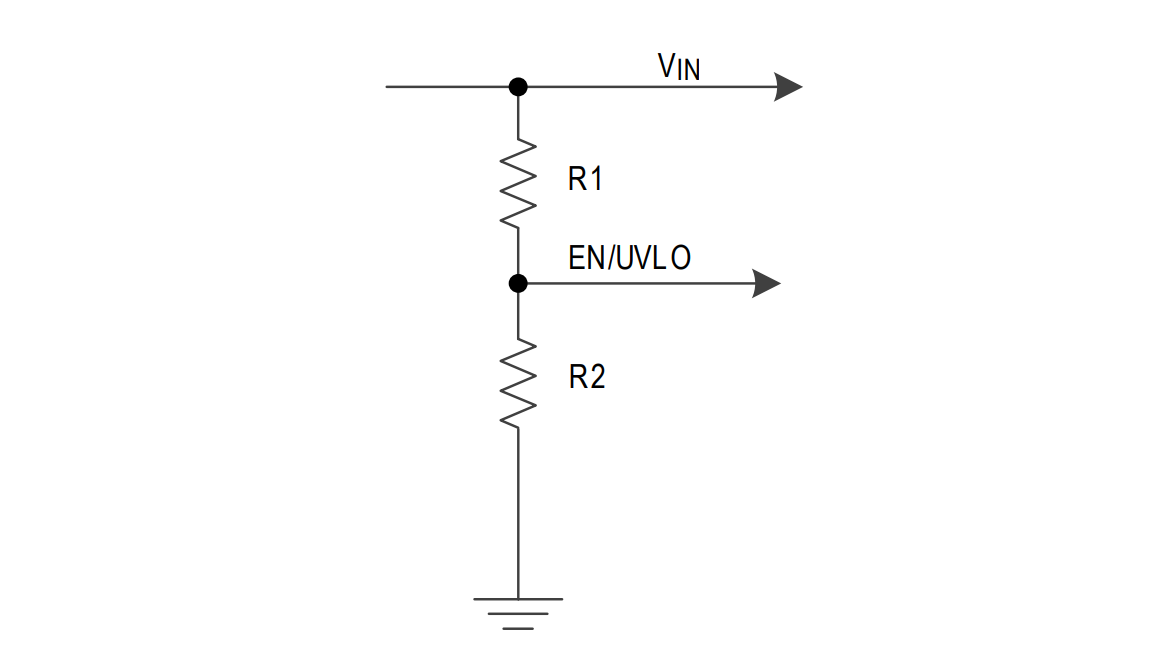
The data sheet recommends a value of 3.3MΩ for R1. R2 is calculated to produce a UVLO of 5.9V using the following equation:
R2 is selected as 866kΩ for this design, which sets UVLO to 5.86V.
- CIN1 is a large, electrolytic capacitor meant to damp any oscillations caused by a long input power path.
- RAC is included to simplify loop response measurements. This can be replaced with a short.
- RSNUB and CSNUB create an RC snubber to reduce ringing on the output. These component values can be finetuned based on the resonant frequency of the device. A capacitance of 10pF and resistance of 100Ω were selected as general values for the time being to give a ‘good enough’ performance.
Documentation & Resources
-
MAXREFDES1274 Design Files5/11/2021ZIP545 K
-
MAXREFDES1274: 5V, 500mA Buck Converter using the MAX17501F5/11/2021PDF386 K
Support & Training
Search our knowledge base for answers to your technical questions. Our dedicated team of Applications Engineers are also available to answer your technical questions.