

Overview
Design Resources
Description
The MAX17559 is a dual-output, synchronous step-down controller that drives nMOSFETs. The device uses a constant- frequency, peak-current-mode architecture. The two outputs can be configured as independent voltage rails. Input capacitor size is minimized by running the two outputs 180° out of phase. The IC supports current sensing using either an external current-sense resistor for accuracy or an inductor DCR for improved system efficiency. Current foldback or latch-off limits MOSFET power dissipation under short-circuit conditions. The IC provides independent adjustable soft-starts/stops for each output and can start up monotonically into a pre-biased output. The IC can be configured in either PWM or DCM modes of operation, depending on whether constant-frequency operation or light-load efficiency is desired. The IC operates over the -40°C to +125°C temperature range and is available in a lead(Pb)-free, 7mm × 7mm, 32-pin TQFP, package.
Features & Benefits
- Wide 4.5V to 60V Input Voltage Range
- Wide 0.8V to 24V Output Voltage Range
- RSENSE or Inductor DCR Current-Sensing
- Fixed 180° Out-of-Phase Operation
- Adjustable 100kHz to 2.2MHz Switching Frequency
- Independent Enable and PGOOD
- Available in a Lead(Pb)-Free 7mm × 7mm, 32-Pin TQFP Package
- Enhances Power Efficiency
- Low-Impedance Gate Drives for High Efficiency
- DCM Operation at Light Loads
- Auxiliary Bootstrap LDO
- Operates Reliably in Adverse Industrial Environments
- Independent Adjustable Soft-Start/Stop or Tracking
- Current Selectable Foldback or Latch-off Limits
- MOSFET Heat Dissipation During a Short-Circuit Condition
- Operates Over the -40°C to +125°C Temperature Range
- Output Overvoltage and Overtemperature Protections
Parts Used
Details Section
The MAX17559 is a dual-output, synchronous step-down controller that drives nMOSFETs. The device uses a constant-frequency, peak-current-mode architecture. The two outputs can be configured as independent voltage rails. Input capacitor size is minimized by running the two outputs 180° out of phase. The IC supports current sensing using either an external current-sense resistor for accuracy or an inductor DCR for improved system efficiency. Current foldback or latch-off limits MOSFET power dissipation under short-circuit conditions. The IC provides independent adjustable soft-starts/stops for each output and can start up monotonically into a pre-biased output. The IC can be configured in either PWM or DCM modes of operation, depending on whether constant-frequency operation or light-load efficiency is desired. The IC operates over the -40°C to +125°C temperature range and is available in a lead(Pb)-free, 7mm x 7mm, 32-pin TQFP, package.
Application
- Industrial Power Supplies
- Distributed DC Power Systems
- Motion Contro
- Programmable Logic Controllers
- Computerized Numerical Control
Benefits and Features
Other features include:
- Wide 4.5V to 60V Input Voltage Range
- Wide 0.8V to 24V Output Voltage Range
- RSENSE or Inductor DCR Current-Sensing
- Fixed 180° Out-of-Phase Operation
- Adjustable 100kHz to 2.2MHz Switching Frequency
- Independent Enable and PGOOD
- Available in a Lead(Pb)-Free 7mm x 7mm, 32-Pin TQFP Package
- Enhances Power Efficiency
- Low-Impedance Gate Drives for High Efficiency
- DCM Operation at Light Loads
- Auxiliary Bootstrap LDO
- Operates Reliably in Adverse Industrial Environments
- Independent Adjustable Soft-Start/Stop or Tracking
- Current Selectable Foldback or Latch-off Limits
- MOSFET Heat Dissipation During a Short-Circuit Condition
- Operates Over the -40°C to +125°C Temperature Range
- Output Overvoltage and Overtemperature Protections
A dual output buck converter using MAX17559 is demonstrated for 16V and 24V DC output application. The power supply delivers up to 4A at 16V and 2A at 24V. Table 1 shows an overview of the design specification.
| PARAMETER | SYMBOL | MIN | MAX |
| Input Voltage | VIN | 36V | 51V |
| Frequency | fSW | 350kHz | |
| Output Voltage1 | VOUT1 | 16 | |
| Output Voltage2 | VOUT2 | 24 | |
| Output Current1 | IOUT1 | 0 | 4A |
| Output Current2 | IOUT2 | 0 | 2A |
| Output Voltage Ripple1 | ∆VOUT1 | 1% of VOUT1 | |
| Output Voltage Ripple2 | ∆VOUT2 | 1% of VOUT2 | |
| Output Power1 | POUT1 | 64W | |
| Output Power2 | POUT2 | 48W | |
| Maximum Efficiency 1 | ƞ1 | 95% | |
| Maximum Efficiency 2 | ƞ2 | 95% | |
This document describes the hardware shown in Figure 1. It provides a detailed systematic technical guide to designing a dual output buck converter using the Analog Devices MAX17559 current-mode controller. The power supply has been built and tested, details of which follow later in this document.


The main components of a buck converter are the power switch, which usually comes in the form of a MOSFET, the inductor, and the diode. As the MOSFET is switched on and off, a magnetic field is generated in the inductor. When the switch is on (or closed), current flows into the inductor and through the output. When the switch is off (or open), due to the magnetic field, current still flows from the inductor to the output load. When the transistor switch is on, it supplies the output load with current. Initially, current flow to the load is restricted as energy is also being stored in the inductor. The current in the load and the charge on the output capacitor, therefore, build up relatively slowly compared with the switch-on time of the MOSFET. During the on period there is a large voltage across the diode, which causes it to be reverse-biased. When the transistor switch is off, the energy that had been stored in the inductor's magnetic field is released. The voltage across the inductor is now in reverse polarity, and sufficient stored energy is available to maintain current flow while the transistor is open. The reverse polarity of the inductor allows current to flow in the circuit through the load and the diode, which is now forward-biased. Once the inductor has been drained of the majority of its stored energy, the load voltage begins to fall, and the charge stored in the output capacitor then becomes the main source of current. This leads to the ripple waveform shown in Figure 2.


Proper interleaving of the phases reduces the input, and output ripple-current stress ensures high efficiency by equally sharing the load current. With the MAX17559, there is a 180° out-of-phase operation that reduces stress on the input capacitors. The 180° phase-shift operation between two output channels have the following advantages:
- Reduction of input and output capacitor RMS current
- Lower input-voltage ripple


Design Procedure for Dual-Output Buck Using MAX17559
Step 1: Selection of Switching Frequency
The selection of switching frequency involves a trade-off between efficiency and components size. Low-frequency operation increases efficiency by reducing MOSFETswitching losses and gate-drive losses, but requires a larger inductor and/or capacitor to maintain low output ripple voltage.
The switching frequency of the device can be programmed between 100kHz to 2.2MHz using the RT pin. A resistor RT is connected between the RT pin and GND for the setting of switching frequency. For this design we have selected a switching frequency of 350kHz for both the outputs. The following expression is used to find the required resistor for a given switching frequency.

A typical resistor of 54.9k is used as RRT, RRT = 54.9kΩ
Step 2: Selection of Inductors
Three key inductor parameters must be specified to select the output inductor.
- Inductance (L)
- Inductor saturation current (ISAT)
- DC resistance of inductor (DCR)
The required inductance (L) is calculated based on the ratio of the inductor's peak-to-peak ripple AC current to its DC average current. This is called the inductor ripple current ratio, or LIR. In this design for both the outputs we have selected LIR of 0.3. The switching frequency fSW, input voltage VIN, output voltage VOUT, and selected LIR then determine the inductor value as follows:

D is the duty cycle, which is equal to the ratio of VOUT and VIN. Depending on the variation in the input voltage range, the duty cycle (D1) of the first output (VOUT1) varies from 0.313 to 0.414. Similarly, the duty cycle (D2) of the second output (VOUT2) varies from 0.47 to 0.67. Substituting these in the above expression gives the minimum, typical, and maximum values of inductance L1 and L2 required for the two outputs as follows:

We selected L1 = 47µH and L2 = 22µH, respectively. The minimum inductor saturation current should be greater than the maximum inductor peak current that is given by the following expression:

∆IL_PK-PK(max) is the maximum inductor ripple current and can be calculated as follows:

The maximum inductor ripple currents ∆IL1_PK-PK(max) and ∆IL2_PK-PK(max) for the two outputs can be calculated as follows:

The peak inductor currents for the two outputs can be calculated as follows:

For VOUT1, we selected the Würth Elektronik power inductor 74435572200 of 22µH with a saturation current limit of 11A. Similarly, for VOUT2, we selected the Würth Elektronik power inductor 7447709470 of 47µH with a saturation current limit of 3.8A.
Step 3: Current Sense Resistor Selection
The current-sensing is performed by an external current-sense resistor for both the outputs. The current sense resistors values can be calculated as follows:
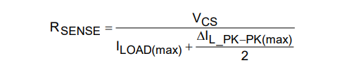
VCS is the selected current sense threshold of 30mV. The current sense resistors for the two outputs can be calculated as follows:

Typical values of 6mΩ and 12mΩ are selected as RSENSE1 and RSENSE2, respectively. The power rating requirements of the selected current sense resistors are calculated as follows:

Substituting values in the above expression, we get:

Step 4: Peak Current Limit Programming
The device features an adjustable peak-current-limit threshold independently for each controller. Connect a resistor from the ILIM_ pin to GND to program the current limit. The resistor value can be calculated using the following expression:

Where ILIM_THRESHOLD can be calculated from the following expression:

For the two outputs ILIM_THRESHOLD can be calculated as follows:

Based on the above results the RILIM for the two outputs can be calculated as follows:

Typical resistor values of 140kΩ are selected as RILIM1 and RILIM2.
Step 5: Setting Output voltages
The output voltage of each output is set by connecting a resistor-divider (comprising resistors R1 and R2) to the FB_ pin from the corresponding output to GND (Figure 4).
Assuming 0.2% offset present on the VOUT we can calculate output voltage offsets for the two outputs. The calculated values of offsets α1 and α2 will be 32mV and 48mV, respectively. The expression below gives maximum possible values of R1 as follows:

Where IFB_ is the maximum leakage current of the FB_ pin and is equal to 0.1µA. The maximum values of R1 for the two outputs can be calculated as follows:

In our design we have selected a typical value of 200kΩ as R1_1 and R1_2.
The value of R2 can be calculated as follows:

The corresponding values of R2 for the two outputs can be calculated as follows:

Typical resistor values of 10.5kΩ and 6.8kΩ are selected for R2_1 and R2_2, respectively.
Step 6: Enable and Setting Input Under Voltage Lockout
The two controllers of the IC can be independently shut down and enabled using the EN1 and EN2 pins. In this design, the EN pins are left unconnected to have both outputs on all of the time. However, if required, a resistor divider can be used to set up the input under voltage lockout level, as explained in the datasheet.
Step 7: Soft-Start
The soft-start/stop time of each controller's output voltage is controlled by the voltage on the relevant SS_ pin for that controller. When the voltage on the SS_ pin is less than the 0.8V internal reference, the device regulates the FB_ voltage to the SS_ pin voltage, instead of the 0.8V internal fixed reference. This allows the SS_ pin to be used to program the output voltage soft-start/stop time by connecting an external capacitor from the SS_ pin to GND. For this design we have set a soft-start time of 10.8ms for both the outputs. The soft-start capacitor value can be calculated based on the following expression:

The soft-start capacitors for the two outputs can be calculated as follows:

A typical capacitor of 68nF is selected as CSS1 and CSS2. A typical resistor of 2kΩ is used in series with both the soft-start capacitors, as stated in the datasheet.
Step 8: Operation Under Current Limit (ILIMSEL)
For this design, latch-off mode is selected for the current limit. Under an overcurrent limit condition, whenever the output voltage drops below 70% of its set value, the controller enters latch-off mode and both the high and low-side MOSFETs are kept off. The latch-off is not active during soft-start. The controller remains idle until the corresponding EN_ pin or the IC supply is cycled to GND and activated again. The ILIMSEL pin of both outputs is connected to GND to configure this mode.
Step 9: Light-Load Current Operation (SKIP)
The MAX17559 can be configured to operate in either discontinuous-conduction mode (DCM) for high lightload efficiency or fixed-frequency pulse-width-modulation (PWM) mode. In this design we have selected the PWM mode of operation under light-load conditions and connected the SKIP pin to VCCINT.
Step 10: Input Capacitor Selection
The input filter capacitor reduces peak currents drawn from the power source and reduces noise and voltage ripple on the input caused by the circuit's switching. For each output channel, the input capacitance required for a specified input-ripple ∆VIN can be calculated using the following expression:

D = Duty Cycle
Ƞ = Target efficiency
∆VIN = Allowed Peak to Peak ripple voltage
For a D = 0.5 (worst case), Ƞ = 95% and ∆VIN = 2% of VINmin the minimum input capacitor values for both the outputs can be calculated as follows:

Considering capacitors derating due to component tolerances, temperature, and DC biasing, 3 x 4.7µF 80V capacitors are used as CIN for both controllers.
Step 11: Output Capacitor Selection
The key selection parameters for the output capacitor are capacitance value, ESR, and voltage rating. These parameters affect the overall stability, output ripple voltage, and transient response. The output capacitor is chosen to have 3% output voltage deviation for a 50% load step of the rated output current. The bandwidth is usually selected in the range of FSW/10 to FSW/20. For the present design, the bandwidth is chosen as FC = 23.33kHz.

The required output capacitance can be calculated from the expression below:

ISTEP is equal to 50% of the full load current for both the outputs. This is equal to 2A and 1A for VOUT1 and VOUT2 respectively. From the above expression, the required output capacitance for the two outputs can be calculated as follows:

A ceramic capacitor of 22µF 25V degrades to 7µF at 16V. Hence five 22µF, 25V capacitors are selected as COUT1 for VOUT1.
Similarly, a ceramic capacitor of 4.7µF 50V degrades to 3.2 µF at 24V. Hence, four 4.7µF, 50V capacitors are selected as COUT2 for VOUT2.
The total ESR of selected output capacitors is as follows:
ESR1 = 0.4mΩ
ESR2 = 0.75mΩ
Step 12: Loop Compensation
The controller uses a peak-current-mode-control scheme that regulates the output voltage by forcing the required current through the external inductor. Current-mode control eliminates the double pole in the feedback loop caused by the inductor and output capacitor, in the case of voltage mode control, resulting in a smaller phase-shift and requiring less elaborate error-amplifier compensation. Typical type-II compensation used with peak current-mode control is shown in Figure 5.


Calculate the compensation resistor RZ using the following expression:

fCO = Cut-off frequency of 23.33kHz
COUT = Worst-case output capacitance, COUT1 = 35µF and COUT2 = 12.8µF
GCS = Current-sense amplifier gain of 12
gM = Internal transconductance amplifier gain of 2m A/V
GFB = Output voltage feedback divider gain of (0.8/VOUT), GFB1 = 0.05 and GFB2 = 0.033
Compensation resistor values for the two outputs can be calculated as follows:

Typical resistor values of 4.12k and 4.42k are selected as RZ1 and RZ2, respectively.
fP_Load is the load pole frequency that can be calculated as follows:

For both outputs, the load pole frequency can be calculated as follows:

CZ is calculated using the following expression:

For both outputs the CZ can be calculated as follows:

A typical capacitor of 33nF is selected as CZ1 and CZ2. The minimum of ESR zero frequency given by the following expression:

For both outputs, the fZ_ESR can be calculated as follows:

Calculate CF using the following expression:

fP_EA is the pole frequency created by RZ and CF, and we set it to the minimum ESR zero frequency calculated above. For both outputs the CF can be calculated as follows:

A typical capacitor of 3.3pF is selected as CF1 and CF2.
Step 13: External MOSFET Selection
- On-resistance RDS(ON)
- Maximum drain-to-source voltage VDS(max)
- Miller Plateau voltage on high side MOSFET Gate (VMIL).
- Total gate charge QGate
- Output capacitance COSS
- Power dissipation rating and package thermal resistance
Both MOSFETs must be logic-level types with guaranteed on-resistance specifications at VGS = 4.5V. A 60V 50A MOSFET BSC067N06LS3 G from Infineon is used as the high-side MOSFET for both outputs. A 60V 45A MOSFET RJK0653DPB-00#J5 from Renesas Technology Corporation is used as the low-side MOSFET for both outputs.
Step 14: Bootstrap Selection
The selected high-side MOSFET determines the appropriate bootstrap capacitance values according to the following expression:

QGate = Total gate charge of high side MOSFET which is 15n C for the selected high side MOSFET
∆VBST = Voltage variation allowed on the high-side MOSFET driver after turn-on. It is selected to be equal to 100m V as advised in the datasheet.
The minimum bootstrap capacitance value for both the outputs can be calculated as follows:

A typical value of 1µF is selected as bootstrap capacitor for both the outputs.
Documentation & Resources
-
MAXREFDES1039 Design Files2/16/2021ZIP4 M
-
EE-Sim OASIS Free Simulator7/9/2019
-
MAXREFDES1039: 64W and 48W Dual Output DC-DC Buck Converter Using the MAX175592/16/2021PDF814 K
Support & Training
Search our knowledge base for answers to your technical questions. Our dedicated team of Applications Engineers are also available to answer your technical questions.