

Overview
Design Resources
Description
This document describes a circuit that uses three MAX17541G buck converters and one MAX17504 step-down DC-DC converter. The circuit is arranged so that each buck converter uses the same input with four separate outputs. Each output has a different power specification. The MAX17541G regulator and features are given first, followed by the MAX17504 features.
MAX17541G
The MAX17541G high-efficiency, high-voltage, synchronous step-down DC-DC converter with integrated MOSFETs operates over a 4.5V to 42V input. The converter can deliver up to 500mA and generates output voltages from 0.9V up to 0.92 x VIN. The feedback (FB) voltage is accurate to within ±1.7% over the -40°C to +125°C operating temperature range. The MAX17541G uses peak-current-mode control with pulse-width modulation (PWM) and operates with fixed 600kHz switching frequency at any load.
MAX17504
The MAX17504 is also a high-efficiency, high-voltage, synchronous step-down DC-DC converter with integrated MOSFETs and operates over a 4.5V to 60V input. The converter can deliver up to 3.5A current. Output voltage is programmable from 0.9V to 0.9 x VIN. The feedback voltage regulation accuracy over -40°C to +125°C is ±1.1.%. The MAX17504 also features a peak-currentmode control architecture. The device can be operated in the pulse-width modulation (PWM), pulse-frequency modulation (PFM), or discontinuous-conduction mode (DCM) control schemes. A programmable soft-start feature allows users to reduce input inrush current. The device also incorporates an output enable/undervoltage lockout pin (EN/UVLO) that allows the user to turn on the part at the desired input voltage level. An open-drain active-low RESET pin provides a delayed power-good signal to the system upon achieving successful regulation of the output voltage.
Features & Benefits
MAX17541G
- Reduced Power Dissipation
- Peak Efficiency > 90%
- Shutdown Current = 0.9μA (typ)
- Operates Reliably in Adverse Industrial Environments
- Hiccup-Mode Current Limit, Sink Current Limit, and Autoretry Startup
- Built-In Output-Voltage Monitoring (Active-Low RESET Pin)
- Programmable EN/UVLO Threshold
- Adjustable Soft-Start and Prebiased Power-Up
- -40°C to +125°C Ambient Operating Temperature Range/-40°C to +150°C Junction Temperature Range
MAX17504
- 100kHz to 2.2MHz Adjustable Switching Frequency with External Synchronization
- Peak Efficiency > 90%
- PFM and DCM Modes Enable Enhanced Light-Load Efficiency
- 2.8μA Shutdown Current
- Operates Reliably in Adverse Industrial Environments
- Hiccup Mode Overload Protection
- Adjustable Soft-Start and Prebiased Power-Up
- Built-In Output-Voltage Monitoring with RESET
- Programmable EN/UVLO Threshold
- -40°C to +125°C Ambient Operating Temperature Range/-40°C to +150°C Junction Temperature Range
Details Section
This document describes a circuit that uses three MAX17541G buck converters and one MAX17504 step-down DC-DC converter. The circuit is arranged so that each buck converter uses the same input with four separate outputs. Each output has a different power specification. The MAX17541G regulator and features are given first, followed by the MAX17504 features.
MAX17541G
The MAX17541G high-efficiency, high-voltage, synchronous step-down DC-DC converter with integrated MOSFETs operates over a 4.5V to 42V input. The converter can deliver up to 500mA and generates output voltages from 0.9V up to 0.92 x VIN. The feedback (FB) voltage is accurate to within ±1.7% over the -40°C to +125°C operating temperature range. The MAX17541G uses peak-current-mode control with pulse-width modulation (PWM) and operates with fixed 600kHz switching frequency at any load. Other features include the following:
- Reduced Power Dissipation
- Peak Efficiency > 90%
- Shutdown Current = 0.9µA (typ)
- Operates Reliably in Adverse Industrial Environments
- Hiccup-Mode Current Limit, Sink Current Limit, and Autoretry Startup
- Built-In Output-Voltage Monitoring (Active-Low RESET Pin)
- Programmable EN/UVLO Threshold
- Adjustable Soft-Start and Prebiased Power-Up
- -40°C to +125°C Ambient Operating Temperature Range/-40°C to +150°C Junction Temperature Range
MAX17504
The MAX17504 is also a high-efficiency, high-voltage, synchronous step-down DC-DC converter with integrated MOSFETs and operates over a 4.5V to 60V input. The converter can deliver up to 3.5A current. Output voltage is programmable from 0.9V to 0.9 x VIN. The feedback voltage regulation accuracy over -40°C to +125°C is ±1.1.%. The MAX17504 also features a peak-currentmode control architecture. The device can be operated in the pulse-width modulation (PWM), pulse-frequency modulation (PFM), or discontinuous-conduction mode (DCM) control schemes. A programmable soft-start feature allows users to reduce input inrush current. The device also incorporates an output enable/undervoltage lockout pin (EN/UVLO) that allows the user to turn on the part at the desired input voltage level. An open-drain active-low RESET pin provides a delayed power-good signal to the system upon achieving successful regulation of the output voltage. Other features include the following:
- 100kHz to 2.2MHz Adjustable Switching Frequency with External Synchronization
- Peak Efficiency > 90%
- PFM and DCM Modes Enable Enhanced Light-Load Efficiency
- 2.8μA Shutdown Current
- Operates Reliably in Adverse Industrial Environments
- Hiccup Mode Overload Protection
- Adjustable Soft-Start and Prebiased Power-Up
- Built-In Output-Voltage Monitoring with RESET
- Programmable EN/UVLO Threshold
- -40°C to +125°C Ambient Operating Temperature Range/-40°C to +150°C Junction Temperature Range
A multiple buck converter circuit using three MAX17541G devices (VOUT1,2,3) and one MAX17504 device (VOUT4) is demonstrated for a single 24V input application. The power supply delivers up to four separate outputs. Table 1 shows an overview of the design specification.
| Parameter | Symbol | Min | Max |
| Input Voltage | VIN | 24V | |
| Frequency | fSW | 600kHz | |
| Efficiency | η | >90% | |
| Output Voltage 1 | VOUT1 | 5V | |
| Output Current 1 | IOUT1 | 300mA | |
| Output Voltage 2 | VOUT2 | 20V | |
| Output Current 2 | IOUT2 | 50mA | |
| Output Voltage 3 | VOUT3 | -20V | |
| Output Current 3 | IOUT3 | 50mA | |
| Output Voltage 4 | VOUT4 | 20V | |
| Output Current 4 | IOUT4 | 2A | |
| Output Voltage Ripple | ∆VOUT | 400mV | |
| Output Current | IOUT | 50mA | 2A |
| Output Power | POUT | 1W | 40W |
This document describes the hardware shown in Figure 1. It provides a detailed systematic technical guide to designing a buck converter circuit using Analog Devices' MAX17541G and MAX17504 current-mode controllers. The power supply has been built and tested, details of which follow later in this document.


The buck converter is the most commonly used type of switching regulator. A switching regulator is a circuit that uses a power switch, an inductor, and a diode to transfer energy from the input to the output of the circuit. These components can be rearranged to form various different topologies of the switching regulator. Feedback and control circuitry is often nested around these circuits to regulate the energy transfer and maintain a constant output. Figure 2 shows a buck converter topology.


In comparison with linear regulators, the main advantage to using switching regulators is that they are far more efficient. Switching regulators can reach efficiencies of over 90%, whereas linear regulators have a typical 40% efficiency rating. There are various types of switching regulators:
- A buck regulator: where voltage is stepped down from input to output.
- A boost regulator: where voltage is stepped up from input to output.
- A buck-boost regulator: where voltage can be stepped up or down from input to output. These can also come in a variety of forms.
The reference circuit portrayed in this document is composed of four buck converters. The 24V input voltage is stepped down to 5V, 20V, -20V, and 20V at outputs 1, 2, 3, and 4, respectively. Buck converters are also useful because while stepping down the voltage, they step up the current, allowing for relatively high output currents to be available. This circuit has a maximum 2A output current.
The MAX17541G and MAX17504 are synchronous buck converters. Synchronous buck converters, as opposed to conventional buck converters, can achieve high efficiency in today’s low-voltage, high-current applications because they replace the catch diode of buck converters with a MOSFET. As a result, the power they dissipate in the off-period is reduced significantly.
In steady-state, the low-side MOSFET is driven such that it is complementary with respect to the high-side MOSFET. This means whenever one of these switches is on, the other is off. In steady-state conditions, this cycle of turning the high-side and low-side MOSFETs on and off complementary to each other regulates VOUT to its set value.
The main components of a buck converter are the power switch, which usually comes in the form of a MOSFET, the inductor, and the diode. As the MOSFET is switched on and off, a magnetic field is generated in the inductor.
When the switch is on (or closed), current flows into the inductor and through the output. When the switch is off (or open), due to the magnetic field, current still flows from the inductor to the output load. This is explained in more detail below.
Transistor Switch “On” Period
When the transistor switch is on, it supplies the output load with current. Initially, current flow to the load is restricted as energy is also being stored in the inductor. The current in the load and the charge on the output capacitor therefore build up relatively slowly in comparison with the switch-on time of the MOSFET. During the on period there is a large voltage across the diode, which causes it to be reverse-biased.
Transistor Switch “Off” Period
When the transistor switch is off, the energy that had been stored in the inductor’s magnetic field is released. The voltage across the inductor is now in reverse polarity, and sufficient stored energy is available to maintain current flow while the transistor is open. The reverse polarity of the inductor allows current to flow into the circuit via the load and the diode, which is now forward-biased. Once the inductor has been drained of the majority of its stored energy, the load voltage begins to fall, and the charge stored in the output capacitor then becomes the main source of current. This leads to the ripple waveform shown in Figure 3.


Design Procedure for the Multiple Buck Converter
Now that the principle of operation of the buck converter is understood, a practical design example can be illustrated. The converter design process can be divided into several stages: power stage design, setup of the current-mode controllers, and the feedback loops. This document is primarily concerned with the power stage designs and the feedback loops, and is intended to complement the information contained in the MAX17541G and MAX17504 IC data sheets. Refer to the IC data sheets for details on how to set up supervisory and protection functions of the controller. The following design parameters are used throughout:
| SYMBOL | FUNCTION |
| VIN | Input Voltage |
| VOUT | Output Voltage |
| ΔVOUT | Output Ripple Voltage |
| IOUT | Output Current |
| fSW | Switching Frequency |
| D | Duty Cycle |
| VINU | Undervoltage Lockout Level |
The above symbols are sometimes followed by parentheses to indicate whether minimum or maximum values of the parameters are intended, for example, minimum input voltage is intended by the symbol VIN(MIN). Unless otherwise noted, typical values are intended.
Step 1: Choosing a Suitable Switching Frequency
MAX17541G
The MAX17541G operates at a fixed 600kHz switching frequency at any load.
MAX17504
The device’s switching frequency can be programmed from 100kHz to 2.2MHz by using a resistor connected from the RT pin to SGND. The switching frequency (fSW) is related to the resistor connected at the RT pin (RRT) by the following equation:

where RRT is in kΩ and fSW is in kHz. Leaving the RT pin open causes the device to operate at the default switching frequency of 500kHz. In this case, a 33.2kΩ resistor was used for RRT to obtain approximately 600kHz switching frequency.
Step 2: Setting the Output Voltage
MAX17541G
The MAX17541G offers an adjustable output voltage from 0.9V to 92% VIN. Set the output voltage with a resistive voltage-divider connected from the positive terminal of the output capacitor (VOUT) to GND. Connect the center node of the divider to the FB pin. To optimize efficiency and output accuracy, use the following procedure to choose the values of R4 and R5 (refer also to the schematics):

Use this method to calculate the feedback resistor values of the two remaining MAX17541G circuits.
MAX17504
Set the output voltage with a resistive voltage-divider connected from the positive terminal of the output capacitor (VOUT) to SGND (see Figure 2). Connect the center node of the divider to the FB pin. Use the following procedure to choose the resistive voltage-divider values: Calculate resistor R19 from the output to the FB pin as follows:

where R19 is in kΩ, crossover frequency fC is in kHz, and the output capacitor COUT is in µF. Choose fC to be 1/9th of the switching frequency, fSW, if the switching frequency is less than or equal to 500kHz. If the switching frequency is more than 500kHz, select fC to be 55kHz. Calculate resistor R19 from the FB pin to SGND as follows:
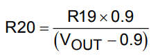
where R20 is in kΩ.
Step 3: Inductor Selection
MAX17541G
Three key inductor parameters must be specified for operation with the device: inductance value (L), inductor saturation current (ISAT), and DC resistance (RDCR). The output voltage determines the inductor value as follows:
L = 8 x VOUT
where L is in µH.
Select a low-loss inductor closest to the calculated value with acceptable dimensions and having the lowest possible DC resistance. The saturation current rating (ISAT) of the inductor must be high enough to ensure that saturation can occur only above the peak current-limit value (IPEAK-LIMIT (typ) = 0.76A for the device).
MAX17504
The same three key inductor parameters must be specified for operation with the device: inductance value (L), inductor saturation current (ISAT) and DC resistance (RDCR). The switching frequency and output voltage determine the inductor value as follows:

where VOUT and fSW are typical values and fSW is in Hz. Select an inductor whose value is nearest to the value calculated by the previous formula. Select a low-loss inductor closest to the calculated value with acceptable dimensions and having the lowest possible DC resistance. The saturation current rating (ISAT) of the inductor must be high enough to ensure that saturation can occur only above the peak current-limit value of 5.25A.
Step 4: Output Capacitor Selection
MAX17541G
X7R ceramic output capacitors are preferred due to their stability over temperature in industrial applications. The output capacitors are usually sized to support a step load of 50% of the maximum output current in the application, so the output voltage deviation is contained to 3% of the output voltage change. The minimum required output capacitance can be calculated as follows:

where ISTEP is the load current step, tRESPONSE is the response time of the controller, ΔVOUT is the allowable output voltage deviation, fC is the target closed-loop crossover frequency, and fSW is the switching frequency (600kHz). Select fC to be 1/12th of fSW. Derating of ceramic capacitors with DC-voltage must be considered while selecting the output capacitor.
MAX17504
The output capacitor selection for the MAX17504 is the same as the MAX17541G. Use the design equations given above to select output capacitor.
In this case, select fC to be 1/9th of fSW if the chosen switching frequency is less than or equal to 500kHz. If the switching frequency is more than 500kHz (as is the case in this circuit), select fC to be 55kHz.
Step 5: Input Capacitor Selection
MAX17541G
The discontinuous input-current waveform of the buck converter causes large ripple currents in the input capacitor. The switching frequency, peak inductor current, and the allowable peak-to-peak voltage ripple that reflects back to the source dictate the capacitance requirement. The device’s high switching frequency allows the use of smaller value input capacitors. X7R capacitors are recommended in industrial applications for their temperature stability. A minimum value of 1μF should be used for the input capacitor. Higher values help reduce the ripple on the input DC bus further. In applications where the source is located distant from the device input, an electrolytic capacitor should be added in parallel to the 1μF ceramic capacitor to provide necessary damping for potential oscillations caused by the longer input power path and input ceramic capacitor.
MAX17504
The input filter capacitor reduces peak currents drawn from the power source and reduces noise and voltage ripple on the input caused by the circuit’s switching. The input capacitor RMS current requirement (IRMS) is defined by the following equation:

where IOUT(MAX) is the maximum load current. IRMS has a maximum value when the input voltage equals twice the output voltage (VIN = 2 x VOUT), so IRMS(MAX) = IOUT(MAX)/2. Choose an input capacitor that exhibits less than +10°C temperature rise at the RMS input current for optimal long-term reliability. Use low-ESR ceramic capacitors with high-ripple-current capability at the input. X7R capacitors are recommended in industrial applications for their temperature stability. Calculate the input capacitance using the following equation:

where D = VOUT/VIN is the duty ratio of the controller, fSW is the switching frequency, ΔVIN is the allowable input voltage ripple, and η is the efficiency. In applications where the source is located distant from the device input, an electrolytic capacitor should be added in parallel to the ceramic capacitor to provide necessary damping for potential oscillations caused by the inductance of the longer input power path and input ceramic capacitor.
Step 6: Setting the Input Undervoltage Lockout Level
MAX17541G
The device offers an adjustable input undervoltage lockout level. Set the voltage at which the device turns on with a resistive voltage-divider connected from VIN to GND. Connect the center node of the divider to EN/UVLO.
Choose R1 to be 3.3MΩ, and then calculate R2 as:

Ensure that VINU is higher than 0.8 x VOUT. If the EN/UVLO pin is driven from an external signal source, a series resistance of minimum 1kΩ is recommended to be placed between the signal source output and the EN/ UVLO pin to reduce voltage ringing on the line.


MAX17504
The MAX17574 uses the exact same procedure as the MAX17541G. In the case of this circuit, all four buck converters use the same voltage-divider to set the UVLO threshold. In this circuit, a 196kΩ resistor is used for R2, setting the UVLO threshold at approximately 21.7V.
Documentation & Resources
-
MAXREFDES1019 Design Files11/8/2021ZIP2M
-
MAXREFDES1019: Multiple-Output, DC-DC Converter using Buck Regulators11/8/2021PDF618 K
Support & Training
Search our knowledge base for answers to your technical questions. Our dedicated team of Applications Engineers are also available to answer your technical questions.