Overview
Product Details
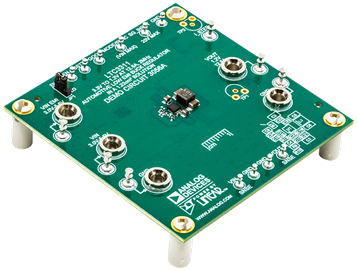
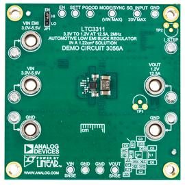
Demonstration circuit 3056A features the LTC3311, 12.5A, low voltage synchronous step-down Silent Switcher® operating as a 2MHz, 2.25V–5.5V input, 1.2V 12.5A output buck regulator. The LTC3311 supports output voltages from 0.5V to VIN with operating frequencies from 500kHz up to 5MHz. The LTC3311 is a compact, ultralow emission, high efficiency, and high speed synchronous monolithic step-down switching regulator. The Silent Switcher technology optimizes fast-current loops and makes it easier to minimize EMI/EMC emissions. Fast minimum on-time of 35ns enables high VIN to low VOUT conversion at high frequency.
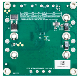
DC3056A is set up to run in forced continuous mode with a 2MHz switching frequency but can be configured to pulse-skipping mode and different switching frequencies. RT is connected to VIN which sets the MODE/SYNC pin as an input and allows the LTC3311 to sync from an external clock. Connecting the MODE/SYNC pin to VIN sets the mode to forced continuous mode and connecting the MODE/SYNC pin to GND sets the mode to pulse-skipping.
Figure 5 in the demo manual shows the efficiency and power loss of the circuit with a 3.3V input in forced continuous mode operation. The DC3056A also has an EMI filter to reduce conducted EMI. This EMI filter can be included by applying the input voltage at the VIN EMI terminal. The EMI performance of the board is shown in the EMI Test Results section. The red lines in Figure 7 through Figure 9 in the demo manual illustrate the CISPR25 Class 5 peak limits for the conducted and radiated emission tests.
The LTC3311 data sheet gives a complete description of the device, operation and application information. The data sheet must be read in conjunction with the demo manual. The LTC3311 is assembled in a 3mm × 3mm LQFN-18 package with exposed pads for low thermal resistance. The layout recommendations for low EMI operation and maximum thermal performance are available in the data sheet section Low EMI PCB Layout.
Markets and Technologies
Applicable Parts
Documentation & Resources
-
DC3056A - Schematic6/30/2021PDF64 K
-
DC3056A - Demo Manual (Rev. 0)6/30/2021PDF903 K
-
DC3056A - Design Files6/30/2021ZIP1 M


