3.3V Lithium-Ion-Cell Buck/Boost Supply Requires One Inductor
Abstract
A combination boost plus LDO (MAX1701) provides a simpler high-performance alternative to single-ended primary inductance converter (SEPIC) and flyback circuits in buck-boost applications
Because lithium-ion batteries and 3.3V power supplies have become so popular recently, portable-equipment designers often must create a 3.3V supply powered by a single Li+ cell. The fact that the output of a Li+ battery ranges above and below 3.3V during its discharge cycle complicates the design.
This situation calls for a special circuit called a "buck/boost converter," which is capable of both step-up and step-down conversions. Portable-equipment engineers have had a similar problem for years in deriving 5V from the output of four nickel-cadmium cells, so the buck/boost requirement is nothing new.
The use of a flyback converter is tempting, but the size and the expense of a transformer and the extra noise created by this converter type prompts the search for an alternative. The single-ended primary inductance converter (SEPIC), for instance, is quieter, but that buck/boost circuit has limited efficiency (usually 85% at best) and requires either a transformer or two inductors (versus the single inductor required by most DC-DC converters).
The third alternative can easily be overlooked, given its use of a linear regulator and the efficiency hit taken when the lithium-ion battery is fully charged (to about 4.2V). Nevertheless, this approach (Figure 1) offers a longer battery life than do the other two buck/boost circuits. For a large portion of the lithium-ion battery's discharge cycle, battery voltage is within a range for which this converter exhibits excellent efficiency.

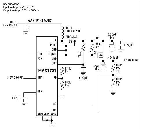
Figure 1. This buck/boost circuit assumes the buck (linear regulator) mode for inputs above 3.3V and the boost (switching regulator) mode for inputs below 3.3V.
The operation of the circuit in Figure 1 is straightforward. When the input voltage is above 3.3V, the IC stops switching and the input voltage is stepped down to 3.3V by a linear regulator comprising Q1, R1, R2, R3, and an op amp internal to the IC. When the input is below 3.3V, the IC operates as a step-up switching regulator and boosts the output to 3.3V. For this condition, the MOSFET is fully on, offering a virtual short from drain to source.
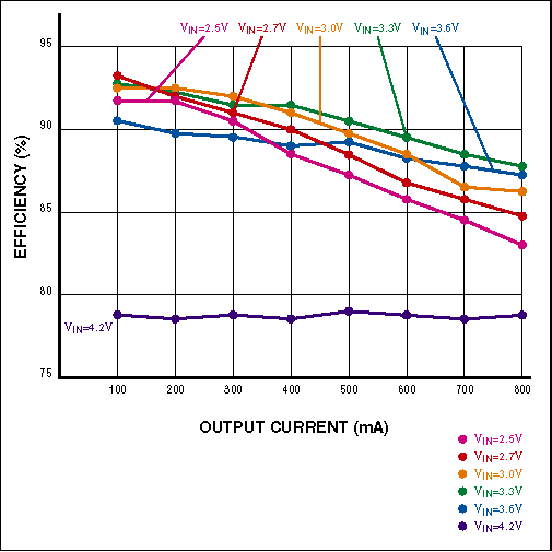
As expected, the efficiency is a minimum for battery voltage at its 4.2V peak (Figure 2). For a 3.6V input and output currents less than 500mA, however, the efficiency is above 89%. This behavior is significant, because the output of a lithium-ion cell is near 3.6V for most of its discharge cycle. For inputs ranging from 3.3V to 3.6V, the efficiency is even better. Efficiency is also excellent when the IC operates as a step-up switching converter, which it does for battery voltages below 3.3V.

Figure 2. Efficiency for the circuit in Figure 1 varies with input voltage and load current, but it assumes a constant minimum when the input voltage is maximum (4.2V).