AN-2625: Designing with Multiple ADE ADCs
Introduction
This application note outlines how to design and configure a system with multiple ADE ADCs.
Supported Devices
Configurations
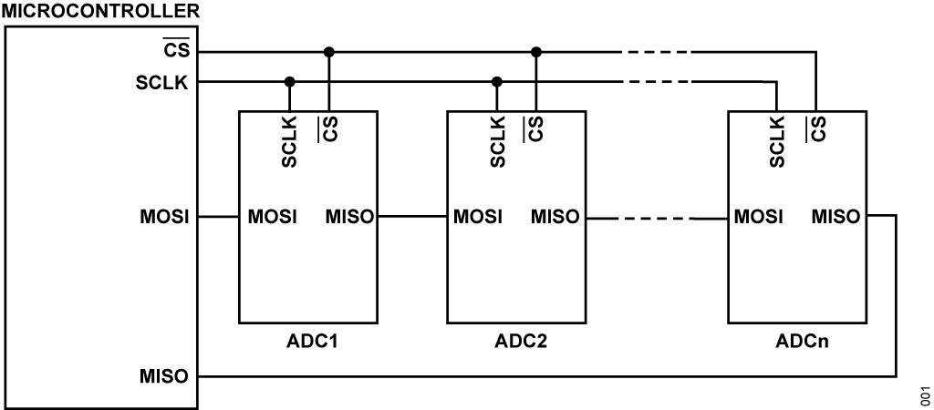
Daisy-Chain SPI
Requirements
The following list outlines the requirements for a daisy chained SPI configuration:
- All devices must operate from the same clock source.
- Single chip select (CS) must be used for all devices.
- Only data ready (DREADY) output from a single device is required.
- See the Data Ready Pin (DREADY) section for more information.

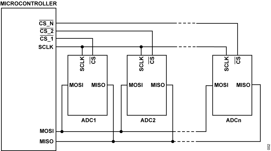
Multi Chip-Select SPI
Requirements
The following list outlines the requirements for a multi chip-select SPI configuration:
- Separate chip select must go to each device.
- See the following if ADC synchronization is required:
- All devices must operate from the same clock source.
- All CS lines must be able to synchronously toggle.
- Only single DREADY output is needed.
- See the following if ADC synchronization is not required:
- All devices can be operated from different clock sources.
- CS lines do not need to be synchronized.
- All DREADY outputs must be brought to the microcontroller separately.
- See the Data Ready Pin (DREADY) section for more information.

Design/Software Considerations
The following sections outline some design considerations to make note of when designing a board with multiple ADCs.
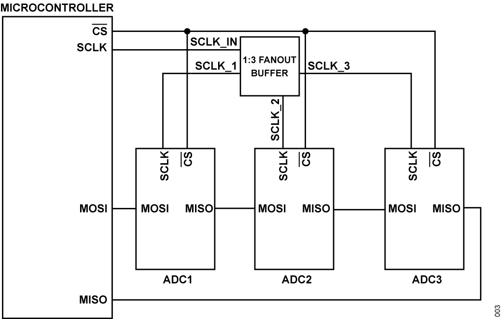
Buffering SPI SCLK
If multiple ADCs are spaced over a large distance, it is recommended to use a 1:x fanout buffer where x is the number of ADCs in the chain. This removes branching of the SCLK trace which may cause reflections and signal integrity issues at high SPI speeds. It also reduces the max length that any single trace needs to cover. For high SPI speeds, use a fanout buffer with low latency; see Figure 3.

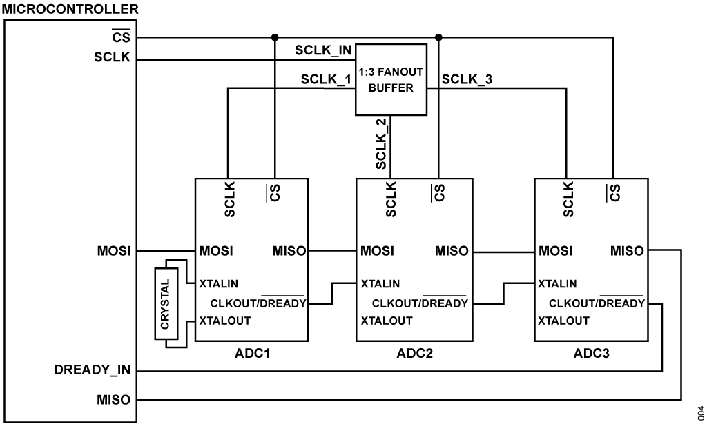
Buffering MCLK
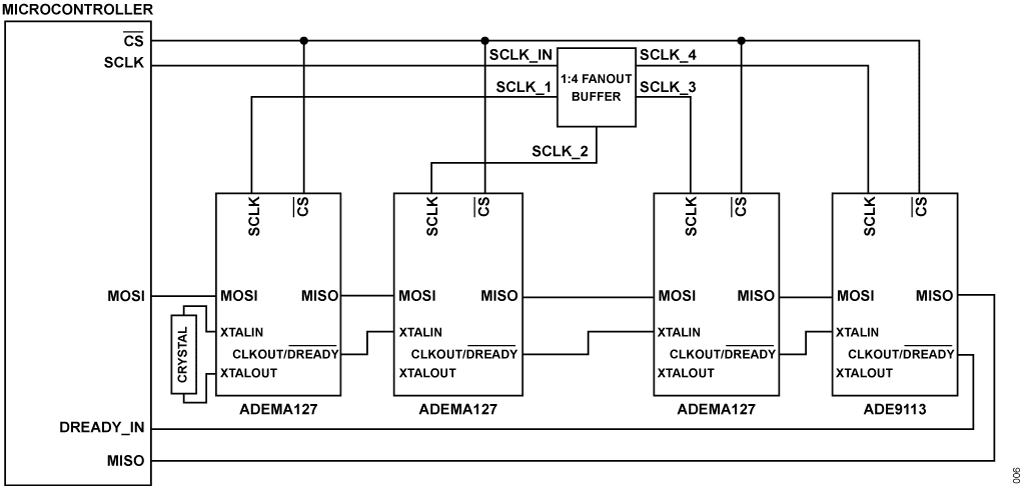
Similar to buffering the SPI SCLK (see the Buffering SPI SCLK section), it is recommended to buffer the MCLK signal to reduce branching and trace length. There are two ways of doing this, using a low latency fanout buffer same as the SPI SCLK or using the ADCs to buffer their own clocks. All supported ADCs (ADEMA12x and ADE91xx) have the functionality to output the MCLK on the CLKOUT/DREADY pin (see the Supported Devices section for more information). In Figure 4, the ADC1 has a crystal connected to its XTALIN/XTALOUT pins generating the MCLK. ADC1 and ADC2 are then configured to output the MCLK on its CLKOUT/DREADY pin which feeds the XTALIN on the next device. The last device in the chain (ADC2 in this case) is configured to output DREADY (data ready) which is fed to the MCU to signal to MCU when new data is ready to be read back from the ADCs.
Note that if there is an ADE91xx device in the chain, avoid using it as the clock source (ADC1 in Figure 4). Use ADEMA12x to supply the clock.

ADC Synchronization
When multiple ADCs are connected to the same SPI bus, the ADC sampling can be synchronized over all devices to ±1MCLK cycle. All ADCs need to be running off the same MCLK source and at the same output data rate. In a multiple chip select configuration, all chip select lines must be able to be simultaneously asserted low. For more information on synchronization of multiple ADCs, see the Synchronization of Multiple Devices section of the ADEMA124/ADEMA127 data sheets and the Synchronizing Multiple ADE9103/ADE9112/ADE9113 Devices section of the ADE9103/ ADE9112/ADE9113 data sheets. Also, see the Sync/Snap Procedure section in this application note for a step by step guide on how to do the synchronization.
Things to Note When Using ADEMA124/ ADEMA127 in the Daisy Chain
If an ADEMA124 or ADEMA127 device is a part of the daisy chain, any time the DATAPATH_CONFIG_LOCK is toggled the ADC conversion is halted and resumed (see the Configuration Lock and Access Bit section of the ADEMA124/ADEMA127 data sheets for more information) which may cause the synchronization between ADCs to be lost.
Two solutions to ensure ADC synchronization is kept after toggling the DATAPATH_CONFIG_LOCK are discussed in the following sections.
Solution 1 (Recommended)
Resynchronize all ADCs after toggling the DATAPATH_CONFIG_LOCK of any device. This solution works for all combination of devices (ADEMA12x and ADE91xx). This method is supported by the ADC service. The energy ADC service provides a set of APIs to communicate with ADI metering ADCs. Link to ADC service: https://github.com/analogdevicesinc/energy-adc-service.
Solution 2
If all devices in the chain are ADEMA12x, then ADC synchronization can be kept if the DATAPATH_CONFIG_LOCK is disabled and reenabled using single SPI transactions, that is all devices are unlocked and locked synchronously. This method is not implemented in the ADC service.
Sync/Snap Procedure
This section outlines a step by step guide on how to perform ADC synchronization and confirm alignment in both the daisy-chain and multi chip-select SPI configurations.
Daisy-Chain SPI Configuration
Align and Measure
The following steps outline how to perform an ADC synchronization and measure to confirm alignment:
1. Write 0x2 to the SYNC_SNAP registers of all devices (0x14).
- Set the ALIGN bit to 1.
2. Read the SNAPSHOT_COUNT_HI (0x17) and SNAPSHOT_COUNT_LO (0x18) registers of all devices.
3. Write 0x1 to the SYNC_SNAP registers of all devices (0x14).
- Set the SNAPSHOT bit to 1.
4. Read the SNAPSHOT_COUNT_HI (0x17) and SNAPSHOT_COUNT_LO (0x18) registers of all devices .
5. Compare the postsync SNAPSHOT_COUNT_x registers of each ADC to confirm synchronization was performed correctly.
- Values must be within ±1 counts.
Measure Only
1. Write 0x1 to the SYNC_SNAP registers of all devices (0x14).
- Set the SNAPSHOT bit to 1.
2. Read the SNAPSHOT_COUNT_HI (0x17) and SNAPSHOT_COUNT_LO (0x18) registers of all devices.
3. Compare the SNAPSHOT_COUNT_x registers of each ADC to confirm synchronization.
Multi Chip-Select SPI Configuration
Align and Measure
The following steps outline how to perform an ADC synchronization and measure to confirm alignment:
1. Write 0x6 to the SYNC_SNAP registers of all devices (0x14).
- Set the ALIGN bit to 1.
- Set the PREP_BROADCAST bit to 1.
2. Read the SNAPSHOT_COUNT_HI (0x17) and SNAPSHOT_COUNT_LO (0x18) registers of all devices simultaneously.
- It is important that the CS of all devices goes from high to low simultaneously.
3. Write 0x5 to the SYNC_SNAP registers of all devices (0x14).
- Set the SNAPSHOT bit to 1.
- Set the PREP_BROADCAST bit to 1.
4. Read the SNAPSHOT_COUNT_HI (0x17) and SNAPSHOT_COUNT_LO (0x18) registers of all devices simultaneously.
5. Compare the postsync SNAPSHOT_COUNT_x registers of each ADC to confirm synchronization was performed correctly.
- Values must be within ± 1 counts.
Measure Only
Measure only can be used to periodically measure the synchronization between ADCs. Allows application to resynchronize if the synchronization has gone outside expected limits.
1. Write 0x5 to the SYNC_SNAP registers of all devices (0x14).
- Set the SNAPSHOT bit to 1.
- Set the PREP_BROADCAST bit to 1.
2. Read the SNAPSHOT_COUNT_HI (0x17) and SNAPSHOT_COUNT_LO (0x18) registers of all device.
3. Compare the SNAPSHOT_COUNT_x registers of each ADC to confirm synchronization.
Data Ready Pin (DREADY)
Each of the supported ADCs has a data ready pin (DREADY) named CLKOUT/DREADY. As the name suggests, this pin can be configured to output the MCLK or the data ready signal. The data ready signals high to low transition indicates when new ADC data is ready to be read from the ADC. The frequency of this signal depends on what data rate the ADC is running at (see the Supported Devices section for more information). To synchronize, all ADCs must be running off the same MCLK source and at the same data rate. Therefore, if ADEMA12x and ADE91xx ADCs are used together in daisy-chain configuration only certain data rates are supported (see Table 1). Once all ADCs are synchronized (see the ADC Synchronization section) all devices data ready are synchronized. Therefore, only one DREADY output signal is needed to be brought to the host MCU. If no ADC synchronization is required all DREADY pins must be brought to the microcontroller.
| Data Rate | ADEMA12x2 | ADE91xx2 |
| 64ksps | X | |
| 32ksps | X | X |
| 16ksps | X | |
| 8ksps | X | X |
| 4ksps | X | X |
| 2ksps | X | X |
| 1ksps | X | X |
| 500sps | X | |
| 250sps | X |
Max ADC Sample Rate in Daisy-Chain Configuration
In a daisy-chain configuration, all ADCs share the same SPI bus. Therefore, the more ADCs that are in the chain, the more data the SPI frame has to transmit. Because of this, there is a limitation to the max output data rate that can be supported for a certain SPI speed and ADC count. All ADCs must be configured to output data in long format (see the Supported Devices section for more information). If SPI isolators are required, make sure to include the propagation delay of the isolator to the calculations (see AN-1478 Application Note, Isolated SPI Bus for Distinct System Requirements for more details on considerations when using isolators).
See the following calculations:
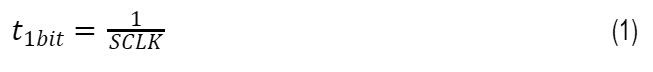
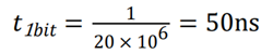
1. Calculate the 1 bit time. This is the time in seconds for 1 bit to be transmitted.
2. Calculate the frame length. This is the length of the entire frame that is transmitted in bits.
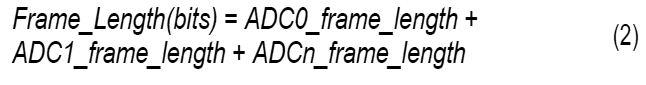
| ADC | Frame Length (bits) |
| ADEMA124 | 160 |
| ADEMA127 | 256 |
| ADE9113 | 128 |
| ADE9112 | 128 |
| ADE9103 | 128 |
3. Calculate the response rate. This is the minimum sample rate needed to support the desired configuration in samples per second.
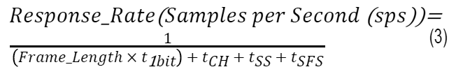
where
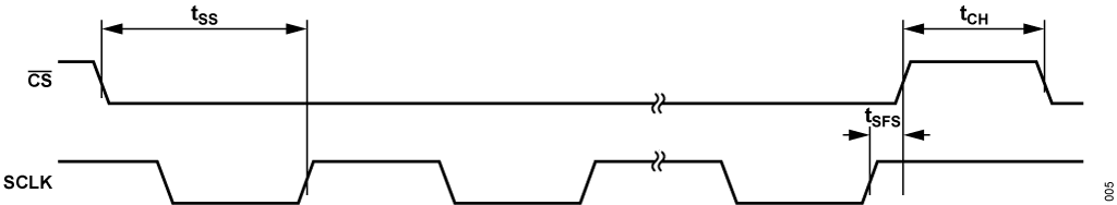
tCH = CS high time between SPI transactions (ns).
tSS = CS to SCLK positive edge (ns).
tSFS = CS high time between SPI transactions (ns).
4. Use look up table to choose supported data rate (see Table 1 for supported data rates).

Worked Example
4 ADCs in the chain: one ADE9113 + three ADEMA127 where
SCLK = 20MHz, tCH = 5000ns, tSS = 10ns, and tSFS = 10ns.
See calculations as follows:
1.
2. Frame_Length = 128 + 256 + 256 + 256 = 896 bits
3.
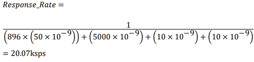
4. When using the ADE9113 and ADEMA127 together only certain data rates are supported. Therefore, the max data rate supported is 8ksps as ADE9113 does not have a 16ksps option.
| Data Rate | ADEMA12x1 | ADE91xx1 |
| 64ksps | X | |
| 32ksps | X | X |
| 16ksps | X | |
| 8ksps | X | X |
| 4ksps | X | X |
| 2ksps | X | X |
| 1ksps | X | X |
| 500sps | X | |
| 250sps | X |
Example
The following section shows an example of a daisy-chain configuration for one ADE9113 and three ADEMA127.
Hardware Setup
Connect the host microcontroller to the four ADCs as shown in Figure 6.

ADC Configuration
The following list outlines how to configure the ADCs for a daisy-chain configuration:
- Configure all the ADEMA127 devices to output MCLK on its CLKOUT/DREADY pin. This is done by writing 0x1 to the CLKOUT_EN bit of the CONFIG0 (0x2) register of the ADEMA127 devices.
Write to first ADC in the chain (device connected to hot MCU MOSI pin), then second ADC, and then the third ADC to ensure that the following ADC has an MCLK before communicating with it. - Configure all devices to have the same output data rate (see the Data Ready Pin (DREADY) section and Max ADC Sample Rate in Daisy-Chain Configuration section for more details.
For ADEMA127, set the output data rate by writing to the DATARATE(0x03C) register (see Output Sample Rate section of the ADEMA124/ADEMA127 data sheets for more details).
For ADE9113, set the output data rate by writing to the DATA-PATH_CONFIG[2:0] bits of the CONFIG_FILT (0x3) register. - Synchronize the ADCs. See the ADC Synchronization section for more details.
Software Configuration
The energy ADC service provides a set of APIs to communicate with ADI metering ADCs. Link to ADC service: https://github.com/analogdevicesinc/energy-adc-service.
Author
