AN-2623: Using the ADF4382/ADF4382A/ADF4383 Fast Calibration Feature for Fast Frequency Hopping Applications
AN-2623: Using the ADF4382/ADF4382A/ ADF4383 Fast Calibration Feature for Fast Frequency Hopping Applications
Introduction
In many phase-locked loop (PLL) frequency generation applications—such as phased arrays and communication systems that use fast frequency hopping—minimizing the time required to switch between frequencies is critically important. The ADF4382/ADF4382A/ADF4383 introduce fast calibration, a feature that significantly reduces total lock time and enables rapid frequency transitions
The ADF4382/ADF4382A/ADF4383 family of PLL devices includes a VCO with two cores and 512 overlapping bands, allowing the device to cover a wide fundamental frequency range. The default method used to select the output frequency uses an internal autocalibration routine which selects the appropriate VCO core and band based on the programmed RF output frequency and the operating temperature. This routine takes a minimum of 100μs for each frequency change.
The total lock time when switching frequencies includes both the autocalibration time and the tuning voltage (VTUNE) settling time within the loop filter. By using fast calibration, the user can bypass the full autocalibration process when switching between VCO bands, significantly reducing the overall lock time.
This application note outlines the fast calibration configuration procedure, explains the theory of operation, and presents example results.
Lock Time Contributors
Phase-locked loop lock time refers to the time taken to lock to a new output frequency from a previous output frequency. During this time, the device is unlocked. An idealized frequency change is illustrated in Figure 1. Lock time consists of both autocalibration time and the VTUNE voltage loop filter settling time.


The starting point for the total lock time measurement is the point at which the frequency begins to change. In the case of the ADF4382/ ADF4382A/ADF4383, this is after a write to the N_INT bit field (Reg 0x010), which triggers a calibration. The frequency begins changing on the last rising edge of the SPI clock signal during this register write, as illustrated in Figure 2.


The point at which a device is considered locked varies depending on the user application specification. For example, the settling threshold parameter used in some applications may be frequency, phase, or tuning voltage settling window. The threshold value used may be 1ppm, 10ppm or a defined frequency or voltage window. For the purposes of standardizing results within this application note, a settling window of 30kHz is used as the settling bandwidth. This means that the device is determined to be locked after it has settled within 30kHz of the final frequency without deviating outside the 30kHz window.


Autocalibration
Autocalibration is the default method for selecting the appropriate core and band value based on the user-defined integer and fractional word. It is enabled by setting EN_AUTOCAL = 1 (Register 0x0020, Bit 7). When a new frequency is set by writing to N_INT (Register 0x0010), the autocalibration routine is triggered. This routine first selects the correct core and then chooses one of 512 bands within the selected core to achieve the desired output frequency. The selected band is based on the temperature of operation (−40℃ to 105℃). For example, when the device operates at a higher temperature, a band corresponding to a higher VTUNE voltage for the output frequency is selected. Likewise, when operating at a lower temperature, a band with lower VTUNE voltage is selected. One advantage of using autocalibration is that, once a selected frequency is locked, it remains locked across the entire operating temperature range of the device (−40℃ to 105℃) without the need to re-run autocalibration. This is known as the lock and leave range.
The default autocalibration time used is 250μs, which is recommended in applications where lock and leave range is more important than reducing lock time. The shortest achievable autocalibration time that still ensures lock and leave performance across temperature is 100μs. Refer to the ADF4382/ADF4382A/ADF4383 data sheets for more information on autocalibration.
Figure 4 illustrates a frequency versus time representation of the core or band selection during autocalibration and subsequent frequency settling within the selected band due to VTUNE voltage settling.


Loop Filter Settling
The VTUNE voltage settling time is dependent on the loop filter component configuration. When a wide loop bandwidth configuration is used, settling time is significantly reduced as compared with using a narrow bandwidth loop filter. An example loop filter is shown in Figure 5. This is designed for FPFD = 250MHz using integer mode output frequencies. Typical VTUNE settling times are less than 10μs using this loop filter. When fractional mode output frequencies are required, additional components are used to reduce sigma-delta modulator (SDM) noise at larger offsets. Larger capacitor values used in the loop filter circuitry result in longer VTUNE settling times.

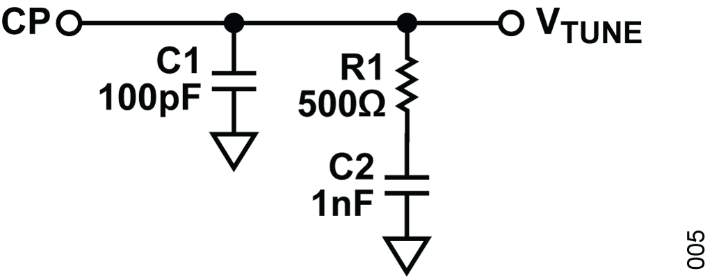
When using fast calibration the VTUNE settling time is the dominant contributor to the overall lock time. The loop filter design should be carefully considered when lock time is a key specification for the system. ADISimPLL can be used to accurately design and model loop filter phase noise response.
Fast Calibration Concept
Fast calibration uses a look-up table (LUT) approach to store the core and band values for 32 points spaced across the octave frequency range of the part. These values are stored during the fast calibration generation stage. To obtain these values, an autocalibration is performed at each of the 32 output frequencies after device initialization (See Fast Calibration Procedure section). This operation is executed automatically when the fast calibration LUT generation step is executed, without the user needing to set each frequency individually. After the LUT generation stage, any frequency change initiated by the user is performed using fast calibration.
Fast calibration performs an interpolation to obtain the correct core and band value between two LUT frequency points based on the user selected frequency. The fast calibration time for each frequency takes <2μs which significantly reduces overall lock time. Figure 6 shows an example plot with 32 LUT points generated across the octave frequency range and the interpolated band values used in fast calibration.


Look-Up Table Scale
The maximum PFD (Phase Frequency Detector) frequency that can be used for generating the LUT is 125MHz. If the required fPFD during normal operation (after LUT generation) exceeds 125MHz, an initial scaled-down PFD frequency of ≤125MHz, referred to as fPFD_LUT, must be used for LUT generation.
PFD_LUT must be set in the reference signal path. This can be achieved by adjusting the reference divider (R_DIV) value accordingly (Register 0x20, Bits[5:0]).
The LUT scale value determines the scaling factor applied to the LUT values and is calculated based on the ratio between the required operational fPFD and the LUT generation fPFD_LUT. The scaling factor is configured via the LUT_SCALE register (Register 0x4F, Bits[7:0]) and is calculated using Equation 1.
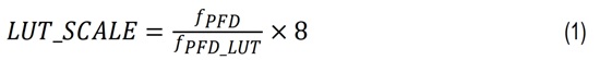
- Example 1: If the user configuration uses fPFD= 125MHz during normal operation, then fPFD = fPFD_LUT. The LUT_SCALE is calculated as:
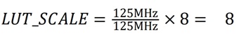
- Example 2: If the user configuration requires fPFD= 250MHz during normal operation, then the 32 LUT points must first be generated at 125MHz. The LUT_SCALE is calculated as:
In this case, R_DIV is incremented to divide by an additional factor of 2 before LUT generation.
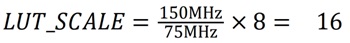
- Example 3: If the user configuration requires fPFD= 150MHz during normal operation, then the LUT table can be generated at 75MHz. The LUT_SCALE is calculated as:
R_DIV must again be incremented to divide by an additional factor of 2 before LUT generation.
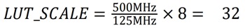
- Example 4: If the user configuration requires fPFD= 500MHz during normal operation, then fPFD_LUT = 125MHz during LUT generation. The LUT_SCALE is calculated as:
In this case, R_DIV is incremented to divide by an additional factor of 4 before LUT generation.
Fast Calibration Procedure


There are 3 main steps to configuring the device for fast calibration. As follows:
- Device Initialization: The device must first be powered up with the necessary supply voltage and initialized by writing register content as per the user configuration. Full register map details are documented on the ADF4382/ADF4382A/ADF4383 data sheets.
- Configure Fast Calibration: After initialization, a 32-point LUT is generated and stored in the device memory. This involves performing an auto calibration at 32 output frequencies across the octave range of the device in order to obtain the core and band information for each frequency. Additionally, this step also updates the VTUNE co-efficient values, sets the appropriate fPFD_LUT for LUT generation by adjusting the reference divider, and sets the LUT_SCALE accordingly.
- Enable Fast Calibration: After the LUT is generated and values stored, fast calibration can be enabled. This involves disabling the auto calibration block and setting the fast calibration enable bit field (EN_LUT_CAL = 1). If fPFD ≠ fPFD_LUT, the reference divider must also be reverted for the user configuration.
The following steps detail the complete fast calibration configuration procedure. This assumes that the device has already been powered up with the necessary power supplies and initialized with the correct register content for the user configuration. The ADF4383 is the variant used in this example with an fPFD= 250MHz.
- Set the VTUNE temperature co-efficient values to the following:
- VPTAT_CALGEN (Reg 0x44 Bits [6:0]) = 0x07
- VCTAT_CALGEN (Reg 0x45 Bits [6:0]) = 0x15
- Determine fPFD_LUT (refer to Look-up Table Scale section). In this example fPFD_LUT = 125MHz, as fPFD= 250MHz is an integer multiple of this.
- Set the R_DIV (Reg 0x020, Bits[5:0]) to divide by an addition factor of 2. In this case, fREF = fPFD during normal operation. Therefore, R_DIV = 2 is the updated value in order to set fPFD_LUT = 125MHz.
- Set EN_LUT_GEN = 1 (Reg 0x36 Bit[1]) to enable look-up table generation.
- Calculate N_INT integer N-value required for the lowest output
frequency (fRFOUT_MIN) in the fundamental range, based on the fPFD and part variant used. For the
ADF4383 the lowest
fundamental output frequency is 10GHz. Therefore:

- Select the lowest RF output frequency by setting
N_INT (Reg 0x10 Bits[7:0] and Reg 0x11 Bits[11:8]) = NMIN =
80.
This step generates the 32 point look-up table for RF output frequencies across the octave range of the device and stores these values within device memory between address 0x201 to 0x273.
Note to set INT_MODE (Reg 0x15 Bit 2) = 1 during this step in order to ensure that the lowest octave output frequency is selected i.e. no fractional word is used from previously written values. - Read FSM_BUSY (Reg 0x58 Bit[1]). The value read back must be 0 to ensure look-up table generation has completed.
- Calculate and set the LUT_SCALE (Reg 0x4F Bits[7:0]) on the
device. As per Look-up Table Scale section:

- Set EN_LUT_GEN = 0 (Reg 0x36 Bit[1]) to disable look-up table generation.
- In the fast calibration configuration procedure it is necessary
to overwrite the last point in the LUT with the core and band
values corresponding to the maximum RF output frequency of
the device. As follows:
- Calculate the maximum N_INT value based on the maximum RF output frequency for the
variant used. For
ADF4383, the maximum output frequency is 20 GHz:
Therefore:

- Set the N_INT (Reg 0x010 Bits[7:0] and Reg 0x11
Bits[11:8]) = NMAX = 160. (INT_MODE = 1).
At this point, an auto calibration is performed which updates the RF output frequency to 20 GHz. - Read back the VCO_CORE (Reg 0x05F Bit[1]) and VCO_BAND (Reg 0x05F Bit[0] and Reg 0x05E Bits[7:0]).
- Write the values read back from VCO_CORE and VCO_BAND in the previous step to M_LUT_CORE (Reg 0x202 Bit[1]) and M_LUT_BAND (Reg 0x202 Bit[0] and Reg 0x201 Bits[7:0]).
- Write M_LUT_N (Reg 0x203 Bits[5:0] and Reg 0x202 Bits [7:2]) = NMAX = 160.
- Set the look-up table address by setting LUT_WR_ADDR (Reg 0x200 Bits[5:1]) = 31.
- Set the override bit field O_VCO_LUT (Reg 0x200 Bit 0) = 1, to override the last bit field in the look-up table with updated band, core and NMAX values.
- Calculate the maximum N_INT value based on the maximum RF output frequency for the
variant used. For
ADF4383, the maximum output frequency is 20 GHz:
Therefore:
- Shutdown CAL_GEN block and clear CAL_VTUNE timeout register by writing PD_CALGEN (Reg 0x2A Bit 0) = 0 and writing CAL_VTUNE_TO (Reg 0x039 Bits[6:0] and Reg 0x038 Bits[7:0]) = 0.
- Revert the R_DIV (Reg 0x020, Bits[5:0]) value back to the original value used upon device initialization for the original configuration of fPFD = 250MHz. i.e. R_DIV = 1.
- Enable fast calibration by setting EN_LUT_CAL (Reg 0x36 Bit
0) = 1.
Fast calibration is now enabled. Lock times will be significantly reduced when changing the RF output frequency.
Note that if ambient temperature varies by more than ±20 ℃ from the temperature that the look-up table is generated, it is recommended to regenerate the look-up table (steps 3 to 12).
Lock and Leave Temperature Range
The lock-and-leave temperature range refers to the span of temperature variation over which the device remains locked—relative to the initial lock temperature—without requiring re-calibration.
When autocalibration is used, the lock-and-leave temperature range is equal to the full operating temperature range, as specified in the ADF4382 /ADF4382A/ADF4383 data sheets. For example, the device remains locked across extreme temperature changes, such as calibrating at −40 °C and continuing to operate if the temperature rises to +105 °C./p>
Using fast calibration, after the 32 point look-up table is generated during initialization, the device remains locked over a narrower temperature range of ±20 °C from the initial temperature. For instance, if fast calibration look-up table generation is performed at 30 °C and the device is locked at 20GHz, the output remains locked at 20GHz between 10 °C and 50 °C. Outside of this temperature range, it is recommended to re-generate the fast calibration look-up table, as otherwise performance may degrade and with larger temperature changes the device may unlock.
Results
The following results show the frequency settling time result of locking between two RF output frequencies. The results are shown in the frequency versus time domain representation. The trigger point for the start of the measurement is the rising edge of the last SPI clock cycle. Autocalibration time is set to a nominal value of 250μs.
The loop filter is configured for a wide loop bandwidth of 1.11MHz in order to reduce the VTUNE settling time component of lock time.


As shown from results, fast calibration has significantly improved lock times for both 11GHz to 12GHz and 12GHz to 15GHz frequency changes. A measurement marker (M1) is placed at the 30kHz settling threshold window which shows lock times of 4.6μs and 1.8μs for these frequency changes. Lock times of less than 10μs are observed across the range of the device with this loop filter configuration and using 30kHz settling window. Lock time variation is based upon the start and stop frequency VTUNE variation and independent of start/stop frequency step size.
| Method | Lock time (μs) | |
| 11GHz to 12GHz | 12 GHz to 15 GHz | |
| Autocalibration | 274 | 274.4 |
| Fast Calibration | 4.6 | 1.8 |
A phase noise comparison is presented in Figure 12 which overlays the phase noise at 20GHz after performing a frequency change using autocalibration (yellow) and fast calibration (blue).
A frequency change is performed from a start frequency of 15GHz to a stop frequency of 20GHz for both autocalibration and fast calibration. The device is populated with the default loop filter design as per the EV-ADF4382SD2Z evaluation board. As shown in the result, there is no degradation in phase noise seen when using fast calibration as compared with the result after using autocalibration.