AN-2168: RF System Development with High-Speed Data Converter
RF System Development Example With Direct RF HSDAC
Our latest high speed data converter chips offer zero IF transceiver architecture combining ADC and DAC with integrated DSP. The 2nd generation 16 nm MXFE supports BW from DC to 18 GHz with max instantaneous bandwidth up to 8 GHz. Such a wide band application necessitates in-depth performance analysis. Additionally, choosing the right component in customer design enables one to optimize linearity and noise performance with adequate unwanted spurious suppression.
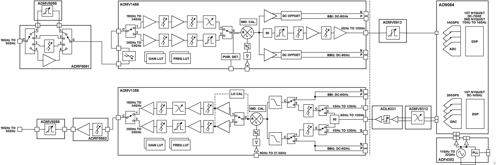
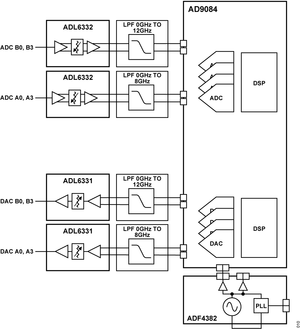
A typical design application incorporates multiple gain and filtering stages cascaded to HSDAC. Moreover, attenuator blocks may be required at various points throughout the RF chain to maintain control over dynamic range, SNR and NSD. Filtering is essential for the purpose of harmonic rejection, out of band noise suppression, channel selection, anti-aliasing or image rejection. A mixer will further enable up and down conversion based on bandwidth requirement. Figure 1 is a block diagram showing our AD9084 HSDAC integrated to TX and RX components for an 18-55 GHz application.
For customers we also offer a less complex reference design with fewer gain and filtering stages integrated to high-speed data converter.

Selecting the Right Amplifier for TX and RX Signal Chain
Amplifier is one of the main building blocks providing in-band gain, reverse isolation and matching while managing noise and linearity. On the TX side the final gain stage often employs a power amplifier, while on the RX side the first gain stage utilizes a Low Noise Amplifier. A power amplifier design is typically optimized for linearity performance to support high power transmission from TX chain. LNA design, on the other hand, is optimized for noise performance since we expect weaker signal at the receiver close to noise threshold.
To select the right Amplifier, we need to consider several RF parameters such as Gain, BW, NF, IP2, IP3, P1dB, common mode rejection, even order harmonic suppression, reverse isolation and input-output return loss.
Need for Image Rejection and Antialiasing Filter
TX Side Filtering
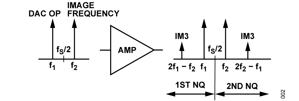
Filters are required on the TX side for DAC image rejection and intermodulation suppression. Consider a single frequency DAC output Fout in the 1st Nyquist zone. This will generate an image Fs-Fout in the 2nd Nyquist zone. If both the image and DAC output frequency fall within the amplifier bandwidth, they act as a two-tone input. This will generate IMD spurious at the output of the amplifier, eventually degrading the SFDR performance of the TX chain.
A lowpass filter will be sufficient for image rejection since we expect image to be at higher frequency. A bandpass filter further suppresses noise and rejects unwanted spurious. When the DAC has differential output one of the key challenges will be to find suitable 50 Ω differential-to-differential filter.

RX Side Filtering
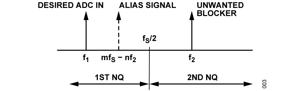
Any unwanted signal input to ADC can alias into desired bandwidth or first Nyquist zone. Therefore, On the RX side a differential anti-aliasing filter is needed before the ADC. This will also reduce unwanted out-of-band noise.

A filter bank or a tunable filter can be employed for this purpose. The ADMV8913 tunable BPF is suitable for x band application.

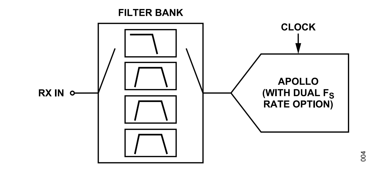
Microstrip filters are fixed bandwidth filters. They are cost-effective, offer less insertion loss and easier to integrate. Tunable active filters, on the other hand, will provide greater bandwidth control but pose challenges in impedance matching and require additional supply and SPI routing.
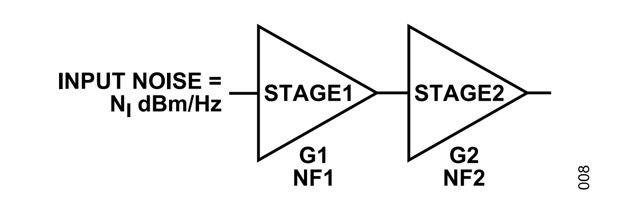
System Optimization and Cascaded Analysis


- For cascaded design define your optimum Pin for each component to satisfy output power, NSD and IP3/IP2 performance across frequency. Also find out your max and min component input level to satisfy constraints and define your operating boundary.
- Determine appropriate attenuator settings for the signal chain. Evaluate TX and RX performance and ensure that any selected device is suitable for system integration.

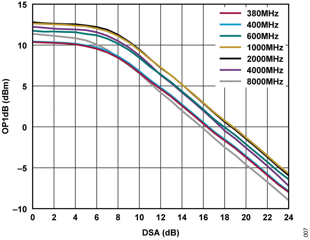
- Take as an example of AD9084 MXFE integration with ADL6331/ ADL6332. The ADL6331 OP1dB is approximately 10 dB at 8 GHz. Maintaining 15 to 20 dB back off from compression the optimal output power will be -5 to -10 dBm. With 14.5 dB gain and 0 dB DSA attenuation the necessary input to ADL6331 ranges from -19 dBm to -24 dBm. Ignoring PCB loss that power will be the required DAC output. As we increase the DAC output the intermodulation products (dBc) will degrade overall SFDR performance. One option to keep your IMD within control is to adjust the attenuation of the built-in DSA for ADL6331. Note that the NF of ADL6331 will rise as we increase DSA attenuation.
- RX path is expected to receive weaker signal closer to noise threshold. If the first stage of RX chain has sufficiently large gain then the impact of noise figure from subsequent stages will be minimal.
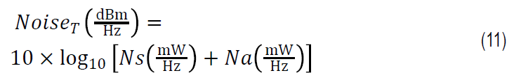
The equation for cascaded noise figure for a 3-stage signal chain :


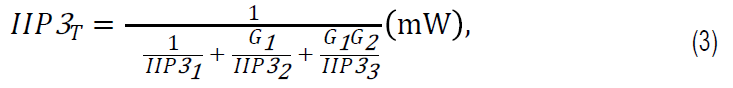
- Conversely RF transmitter deals with high power signal transmission. In a typical cascaded RF design if we can ensure large overall gain it is the final output stage IP3 that will predominate for TX chain.
Equation for Input referred third order intercept point for a 3-stage cascade,


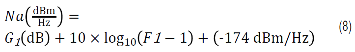
- Cascaded Noise and SNR
Noise contribution from a 2-stage cascade can be calculated as :

Noise output from the first stage due to the input or source noise,

Assume Noise Figure for the first device:

So noise output contributed by the first device in room temperature
While
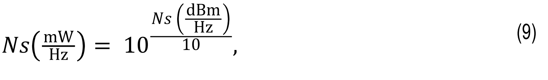
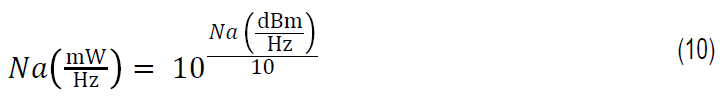
Total Noise Output from first stage
This NoiseT will act as an input to the second stage. NSD for the subsequent stages can be calculated following the same procedure.
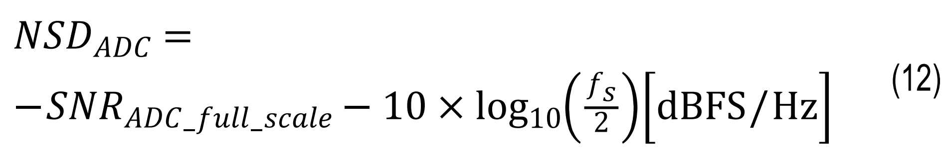
If the full-scale SNR is known for the ADC the NSD for the ADC can be calculated as:
The output SNR at each stage can be calculated with the information from input SNR, device gain and noise figure.


Where

and

A lower noise figure, higher gain and higher IP3 will ensure better output SNR and SFDR. With the help of digital and analog filtering overall noise and spurious contribution can be reduced for the spectrum.
AD9084-FMCB-EBZ Reference Design
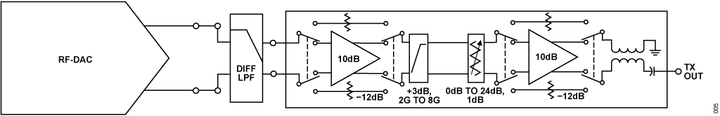
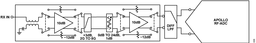
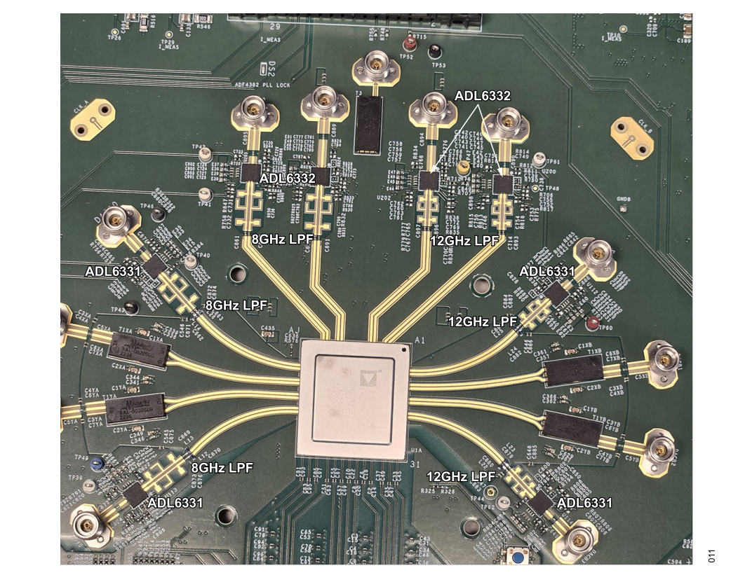
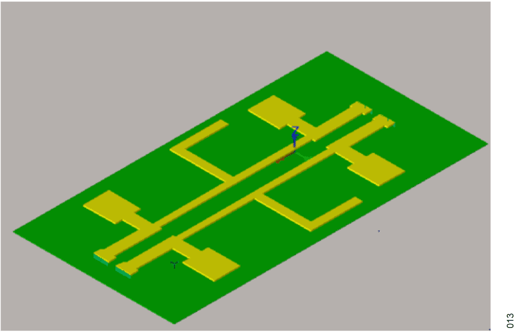
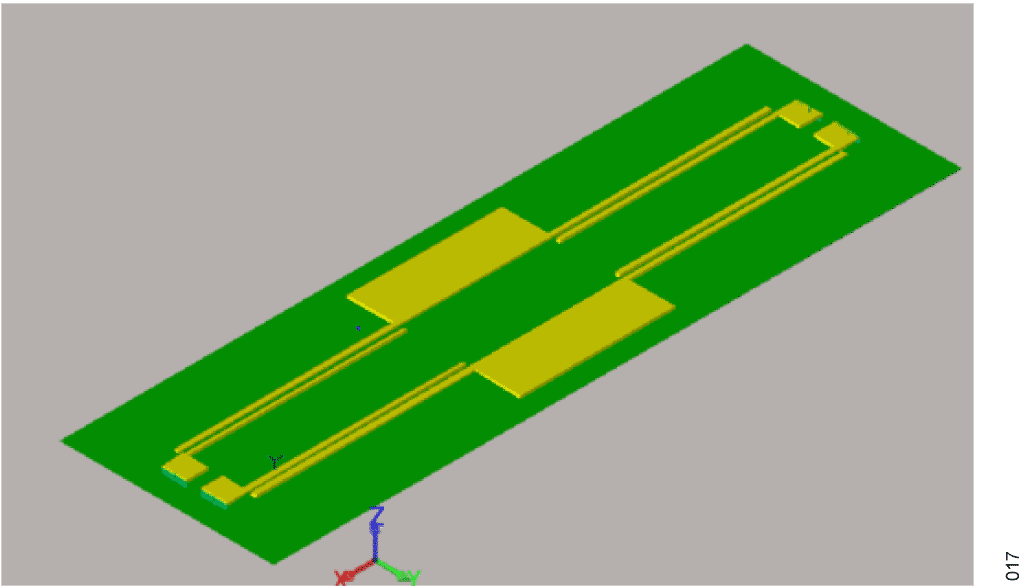
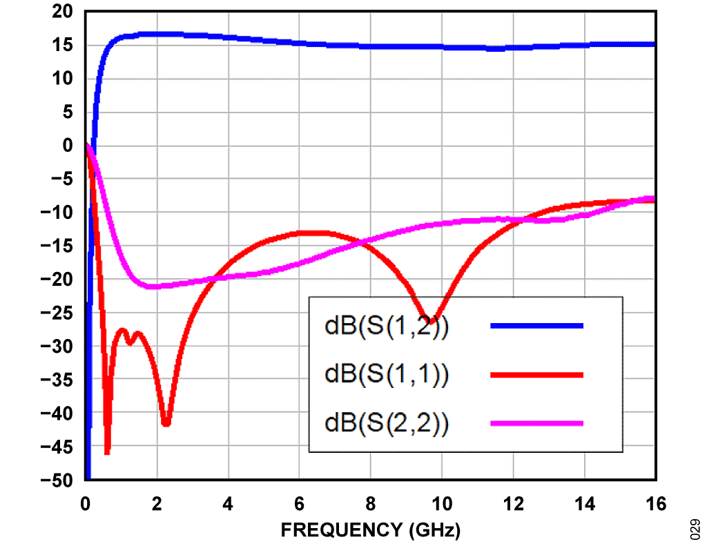
AD9084-FMCB-EBZ rev B reference design is shown in Figure 10. It integrates the AD9084 4T4R high speed differential data converter with differential microstrip lowpass filters and TX/RX variable gain amplifiers ADL6331 and ADL6332. The microstrip filters ensure wideband impedance matching , also provides ease of integration with a fixed cut off frequency.


ADL6331 Integrated to Apollo DAC Output
The ADL6331 presents balanced resistive load to Apollo DAC with differential in -SE out integrated balun. This improves IM2 performance of the DAC compared to the external balun which offers asymmetric impedances across frequency. Minimum impact expected on system NSD and EVM performance.
ADL6332 Integrated to Apollo ADC Input
The ADL6332 offers resistive, balanced source termination to ADC and good reverse isolation minimizing ADC leakage into the front end. The SE in- differential out variable gain amplifier has integrated balun. Minimum impact on system SNR performance.
Filter Selection for the Reference Design
This design incorporates filters with two different cutoff frequencies. In both TX and RX channels, A0 and A3 support L/S/C bands, while B0 and B3 are suitable for X-band applications.


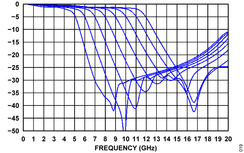
Additional differential high pass and bandpass filters between the VGA and AD9084, as shown in Figure 16 and Figure 17, were also analyzed but not integrated into the reference design.


Tunable differential filters are also suitable for applications up to the X-band. However, integration can be more challenging due to the wideband impedance matching requirements.

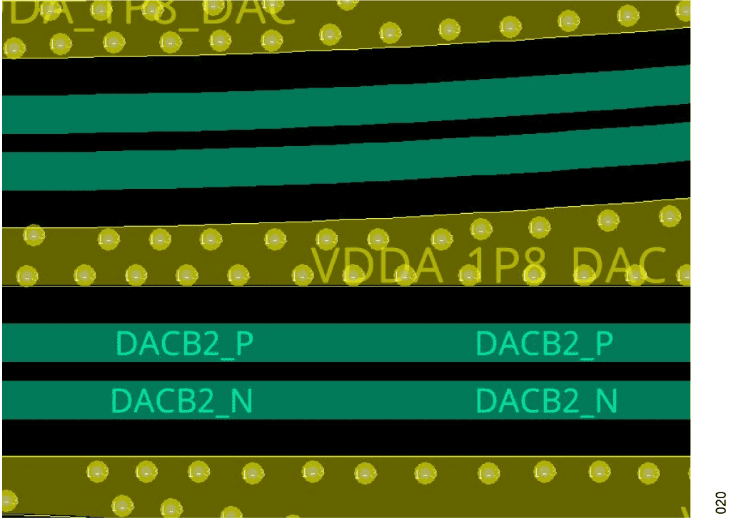
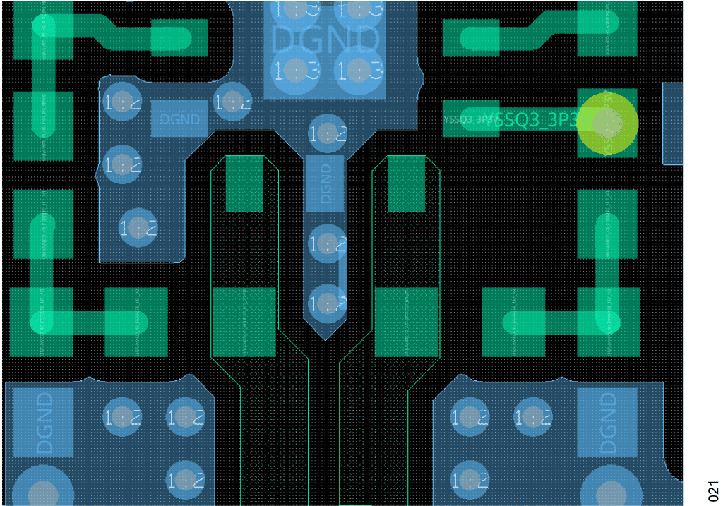
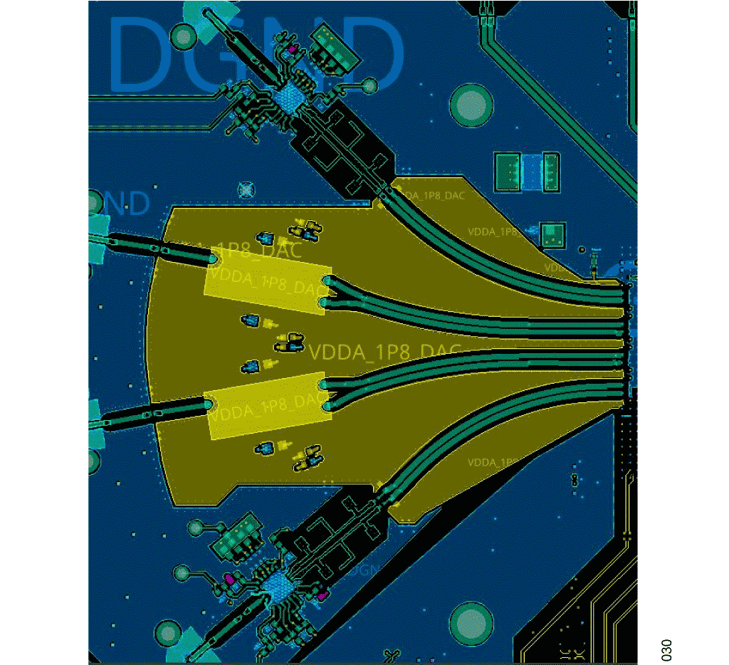
Optimizing PCB Routing for the Reference Design
The Eval board design has all the DAC, ADC and clock traces routed on the top of the PCB as microstrip. It uses a fencing technique with GND vias to provide isolation. To further improve the isolation between the ADC, DAC and the CLK traces the clock traces can be routed at the bottom layer and the ADC/DAC traces can be routed as strip line on L2.
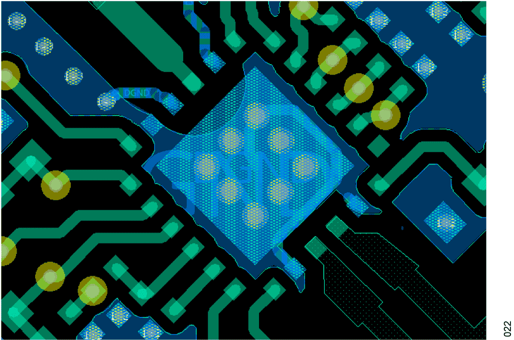
To minimize insertion loss at higher frequencies, consider using low loss PCB materials like Rogers 4003 or Itera MT-40. The distance between components in the cascade should be minimal to prevent sharp gain roll off. Good wideband impedance matching will ensure less ripple in frequency response. Board level electromagnetic (EM) simulation can be performed to optimize return loss.

For differential ADC input or DAC output a differential amplifier or filter may be necessary. When designing the PCB, optimize the transition from differential lines to amplifier pads. Perform EM simulation of your PCB with all pads and discontinuities. A shorter transition is preferrable for low insertion loss and improved return loss across the frequency range.


AD9084-FMCB-EBZ Performance Analysis
TX Side
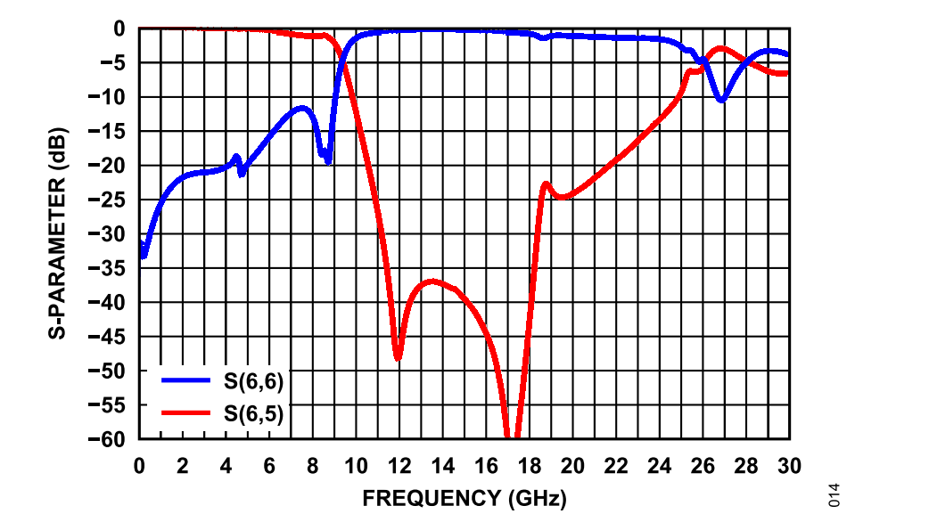
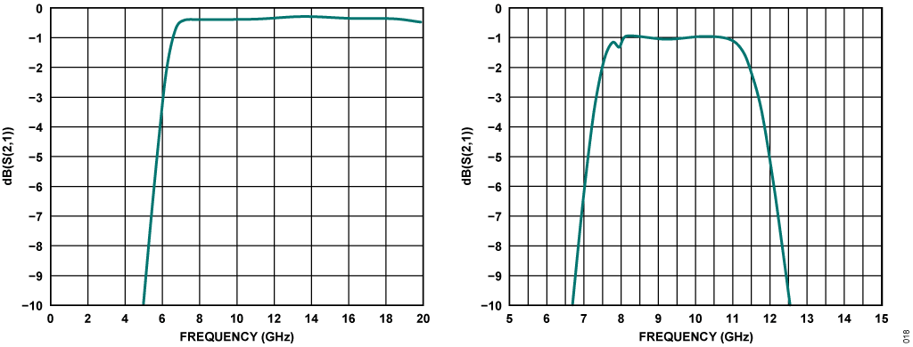
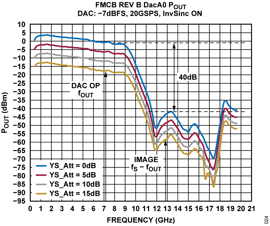
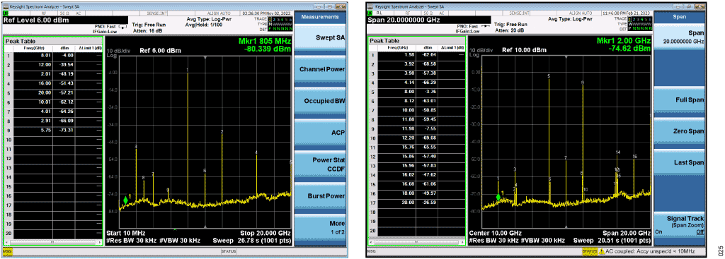
The TX channel data for a 20 Gsps converter sampling frequency is shown in Figure 23. The response of channels A0 and A3 begins to roll off at 9 GHz, achieving 40 dB image rejection in the second Nyquist zone. DAC channels B0 and B3 are optimized for X-band applications. These TX channels are expected to exhibit similar image rejection with 28 Gsps sampling frequency
The ADL6331 VGA features two gain stages with a DSA in between. It provides a nominal gain of 14 dB and a dynamic range of 24 dB. For high-power DAC output signals that are ultimately fed into the first amplifier stage, the DSA can attenuate the signal to enhance overall system performance by reducing harmonics, intermodulation, and spurious emissions.
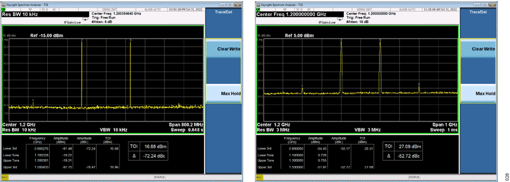
Without proper filtering both the carrier and DAC image could be in-band for the amplifier, and it may create intermodulation distortion. This distortion manifests as unwanted signals across the desired spectrum. Figure 24 illustrates how filtering can effectively remove in-band spurious components, thereby improving SFDR for such a reference design.


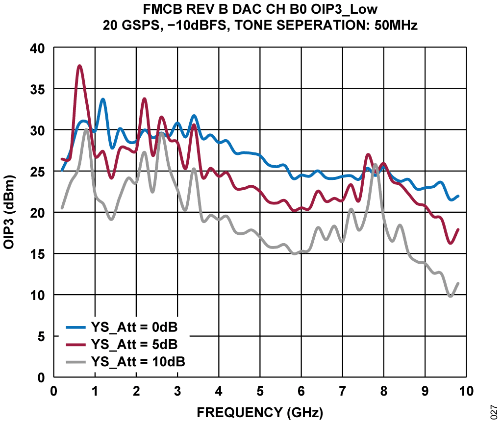
ADL6331 has higher OIP3 compared to DAC output buffer. This will improve the overall OIP3 for the TX chain as shown in Figure 25.


As you increase your DAC output signal power this may drive the final stage amplifier close to compression. To reduce spurious content DSA attenuation can be increased which is placed in between the two amplifier stages of ADL6331.
Cascaded Simulation With Data Converter Model
Transceiver design should be optimized for low in-band insertion loss, enhanced impedance matching and high channel to channel isolation with the help of RF simulation technique. System nonlinear performance also can be assessed with tools like System Vue.
Following approach was taken to optimize the performance of AD9084 FMCB reference design.
- PCB traces, including the discontinuities and component pads, were simulated using EMPro EM simulator.
- S-parameter models were readily available for AD9084 diff MXFE and ADL6331 VGA.
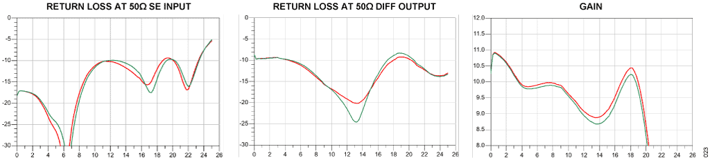
- In the next step combined s-parameter simulation including PCB and RF components was performed with ADS simulator. This will check the return loss across frequency. If necessary, PCB design can be altered at this stage in which case reassessment of EM simulation results will be required.
- AC simulation was conducted at the final step to check Pout, in-band ripple and roll off across bandwidth.
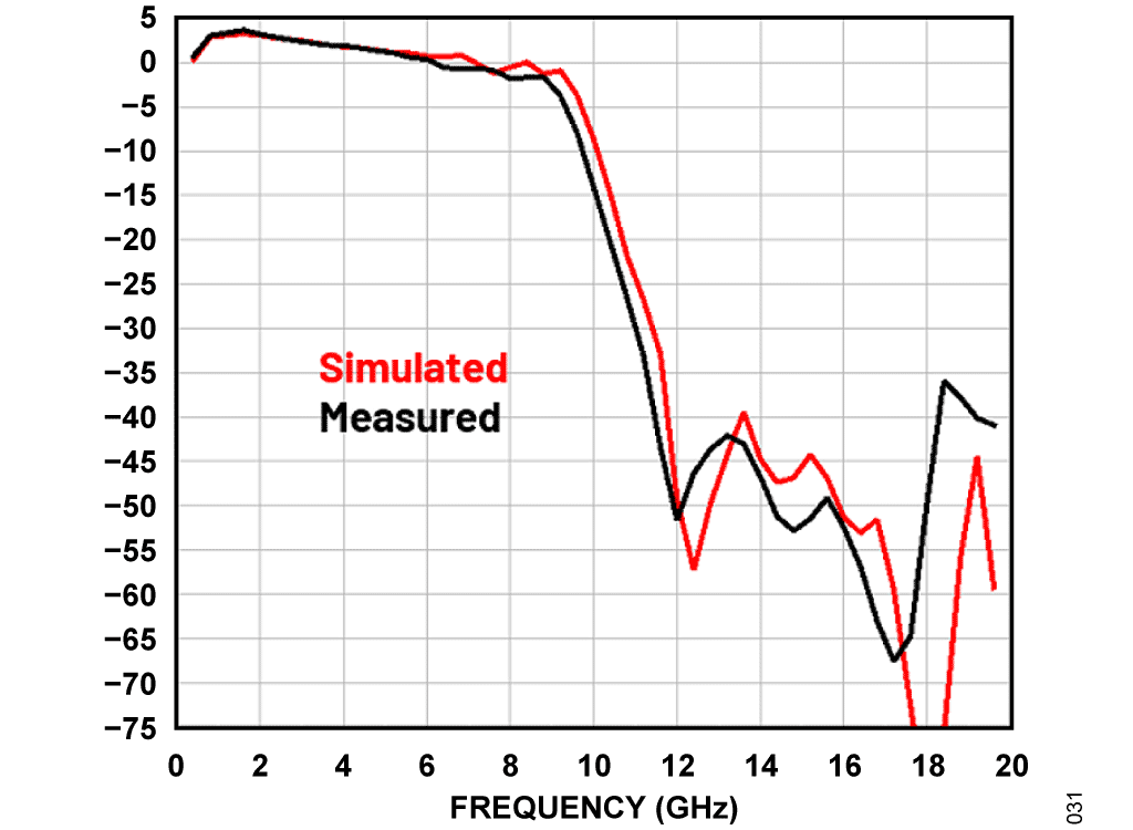
Figure 30 displays the simulated Pout for one of the DAC RF chain which is further compared with the measured data. It demonstrates strong correlation between the measured and simulated data.


RX Side
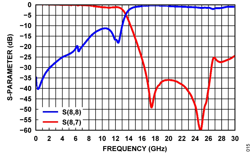
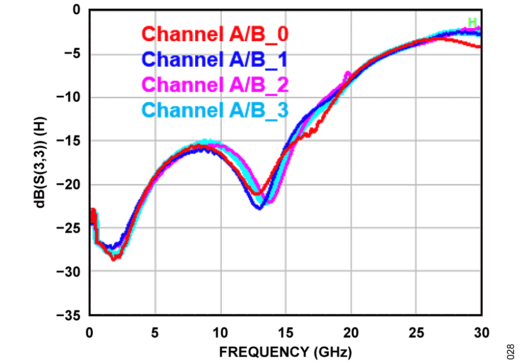
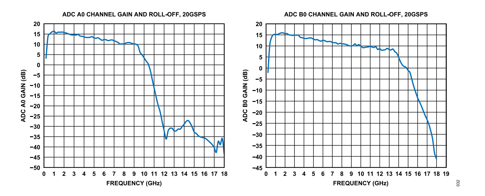
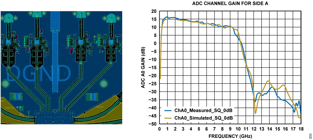
The anti-aliasing filter roll-off is visible from Figure 31. ADC channel Side A supports L/S/C bands, and Side B supports up to X-band. The design is capable of 40dB out-of-band rejection. An additional single-ended high-pass or bandpass filter can be added at the RF connector prior to signal injection, which can provide more selectivity for the RX channel. The filter will also suppress out-of-band noise and thereby improve NSD.


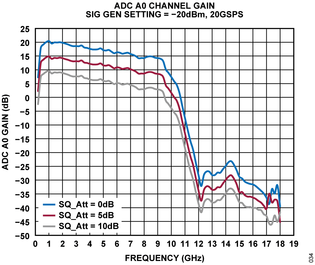
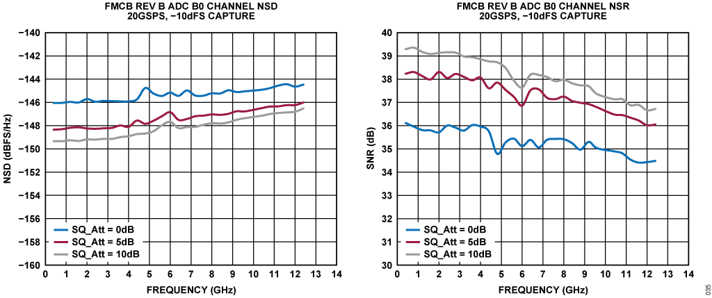
The RX design characterization was performed with a low-noise signal generator (SMA100B), which maintains stable low-noise injection The input signal power was varied for -10 dBFS ADC capture across multiple DSA attenuation levels. In addition to increased dynamic range, the integrated DSA between the two amplifiers of the ADL6332 offers tuning capability to optimize NSD and SNR performance. Suitable operating conditions can be chosen for any signal injection by varying the DSA setting.

Conclusion
This document outlines amplifier selection, PCB routing considerations, filtering strategies, and system-level optimization for RF transceiver designs incorporating high-speed data converters. As an example, TX and RX signal chain optimization techniques are shown for a reference design with AD9084 data converter. By carefully selecting components and employing systematic simulations, designers can achieve optimal linearity, noise performance, and spurious suppression across the RF chain.
Author
