AN-1532: Reconstructive Video Filter for the ADV7393 Video Encoder Using the ADA4430-1 Amplifier
AN-1532: Reconstructive Video Filter for the ADV7393 Video Encoder Using the ADA4430-1 Amplifier
Circuit Function and Benefits
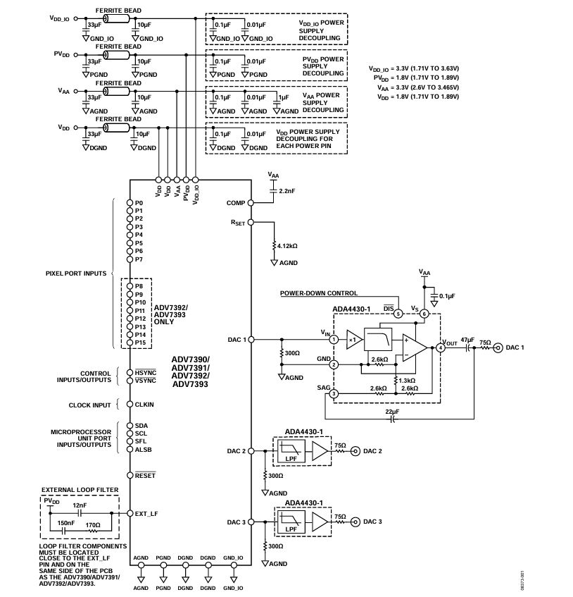
The circuit shown in Figure 1 illustrates a digital-to-analog video converter (video DAC) paired with a low cost, low power, fully integrated reconstruction video filter. Although many video encoders, also known as video DACs, such as the ADV7393 can drive a video load directly, it is often beneficial to use a video driver at the output of a video encoder for power savings, line driving, and additional circuit protection. The video driver is typically configured as an active filter, also known as a reconstruction or anti-imaging filter. The purpose of the reconstruction filter is twofold: it blocks the higher frequency components (above the Nyquist frequency) that are introduced into the video signal as part of the digitization process, and provides gain to drive the external 75 Ω cable to the video display. For ac-coupled output applications, the ADA4430-1 has an integrated signal amplitude gain (SAG) correction network. SAG correction is used to provide low frequency compensation for the high-pass filter formed by the 150 Ω video load of a back terminated cable and the output coupling capacitor. SAG correction reduces the size of the traditionally large ac coupling capacitor (330 µF), replacing it with much smaller 47 μF and 22 μF capacitors.

The ADA4430-1 and the ADV7393 are recommended for automotive applications, which makes both products ideal for infotainment and vision-based safety systems applications.
Circuit Description
The ADV7393 is a low power, fully integrated digital video encoder that converts digital 16-bit component video data, for example, from a complementary metal-oxide semiconductor (CMOS) rearview camera, into a standard analog baseband video signal compatible with worldwide standards. The three 2.6 V/3.465 V 10-bit video DACs provide support for composite (CVBS), S-Video (YC), Component YPrPb, or Component RGB analog outputs in either standard definition (SD) or high definition (HD) video formats. The circuit shown in Figure 1 is configured for low drive output current operation, which reduces the output current by 85% in all three DACs (RSET = 4.12 kΩ, RL = 300 Ω). To further save power, the internal phase locked loop (PLL) is disabled, and the encoder operates in a 2× oversampling mode. The 16-bit video input port is configured to support SD video.
The ADA4430-1 is a single sixth-order, low-pass video filter with a 9.7 MHz (typical) −3 dB cutoff and 50 dB (typical) of out of band rejection at 27 MHz. The ADA4430-1 is a low power, low cost, rail-to-rail output amplifier that has an operating supply range of 2.5 V to 6 V and is ideal for SD video application. Combined with the ADV7393 single chip video encoder, the ADA4430-1 enables the most power efficient video output solution for automotive applications. In Figure 1, the ADA4430-1 is configured as a reconstruction video filter with ac-coupled output with SAG correction. The compensation network includes the C1 and C2 capacitors, and the internal resistor network integrated into the ADA4430-1. Traditional ac coupling uses a large, expensive coupling capacitor, making it costly and wastes valuable printed circuit board (PCB) space. SAG correction allows two small, low cost capacitors to replace the one large ac coupling capacitor and maintain the same field tilt. Field tilt is a measure of the voltage droop (tilt) that occurs on the ac coupling capacitor when a constant luma signal is applied. This droop is caused by the small discharge current created by the 75 Ω load resistor. The SAG correction capacitor values are chosen to achieve the equivalent field tilt of a 220 µF ac coupling capacitor.
When using the SAG correction circuit, the gain from the input to the immediate output of the ADA4430-1 is 2.5 (≈ 8 dB) at extremely low frequencies, where the outer feedback loop formed by the 22 μF capacitor effectively opens (see Figure 2) and exhibits a second-order peak of approximately 11 dB at approximately 5 Hz. This gain is approximately 7.5 dB at 30 Hz. The extra gain must be accounted for when considering low frequency input and output signal swings to keep them within their specified limits. The gain from the ADA4430-1 input to the load side of the 47 μF capacitor does not exhibit this behavior; instead, it appears more like a single-pole, high-pass response.

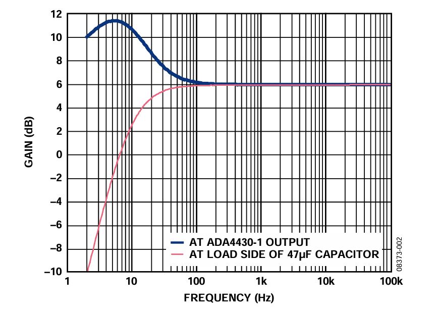
Figure 2 illustrates the SAG frequency response immediately at the ADA4430-1 output and at the load side of the 47 μF capacitor.
Buffering is an important function that is often overlooked. For example, many automotive users use low cost amplifiers to protect more expensive and complex devices, such as video decoders and encoders. Amplifiers with ac-coupled outputs as shown in Figure 1 help protect such devices from overvoltage and electrostatic discharge (ESD) damage.
Common Variations
There are a few options for ac-coupled output configuration. SAG correction, as shown in Figure 1, uses 22 μF and 47 μF capacitors. The traditional ac-coupled output uses a single 220 μF capacitor; in this configuration, the SAG pin is connected directly to the output pin before the output capacitor. For dc-coupled configurations, the SAG pin is also connected directly to the output pin. In both dc-coupled and traditional ac-coupled configurations, connecting the SAG pin directly to the output pin results in a gain of 2 buffer at all video frequencies.
References
Kester, Walt. 2005. Chapter 8 and Chapter 9. The Data Conversion Handbook. Analog Devices, Inc.