AN-1514: Interfacing the ADL5317 High-Side Current Mirror to a Translinear Logarithmic Amplifier in an Avalanche Photodiode Power Detector Application
Circuit Function and Benefits
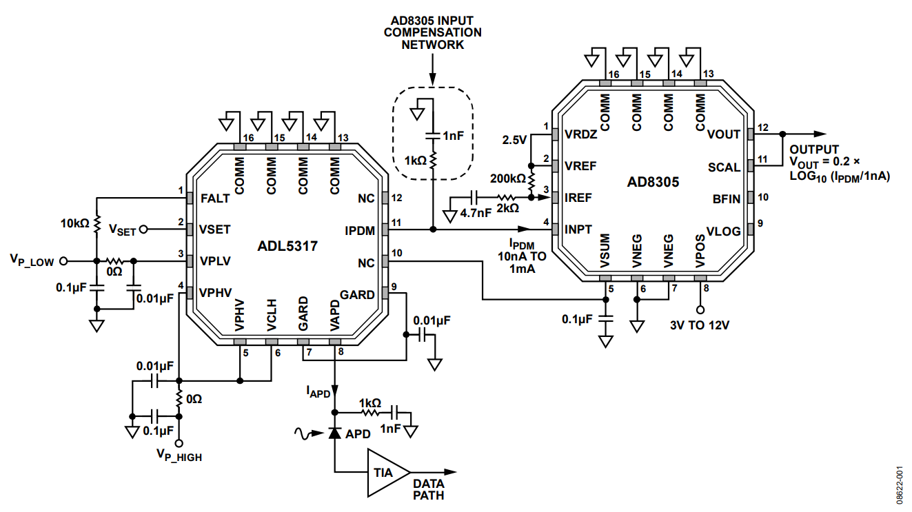
The circuit in Figure 2 uses the monitor current output, IPDM, of the ADL5317 to interface directly to an Analog Devices, Inc., translinear logarithmic amplifier (log amp) such as the AD8304, AD8305, ADL5306, or ADL5310. Figure 2 shows the basic connections necessary for interfacing the ADL5317 to the AD8305. In this configuration, the designer can use the full current mirror range of the ADL5317 for high accuracy power monitoring of an avalanche photodiode (APD).
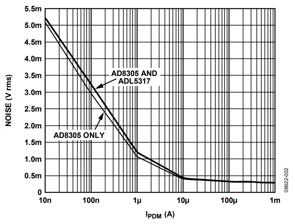
Measured rms noise voltage at the output of the AD8305 vs. input current, IPDM, is shown in Figure 1 for the AD8305 by itself and in cascade with the ADL5317. The relatively low noise produced by the ADL5317, combined with the additional noise filtering inherent in the frequency response characteristics of the AD8305, results in minimal degradation to the noise performance of the AD8305.


Circuit Description
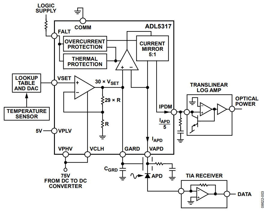
The ADL5317 is primarily designed for wide dynamic range applications that simplify APD bias circuit architecture. Accurate control of the bias voltage across the APD becomes critical to maintain the proper avalanche multiplication factor when the temperature and input power vary. Figure 3 shows how to use the ADL5317 with an external temperature sensor to monitor the ambient temperature of the APD. Using a lookup table and digital-to-analog converter (DAC) to drive the VSET voltage, it is possible to apply the correct VAPD for the conditions. Note that all connections to the ADL5317 are not shown for clarity.
In this application, the ADL5317 operates in linear mode. The bias voltage to the APD, delivered at the VAPD pin, is controlled by the voltage (VSET) at the VSET pin. The bias voltage at VAPD is equal to 30 × VSET.
The range of voltages available at the VAPD pin for a given high voltage supply is limited to approximately 33 V (or less, for VAPD < 41 V). This limitation is because the GARD and VAPD pins are clamped to within ~40 V below VPHV, preventing internal device breakdowns.
The input current, IAPD, is divided by a factor of 5 and precisely mirrored to the IPDM pin. This interface is optimized for use with any of the Analog Devices translinear logarithmic amplifiers (for example, the AD8304 or AD8305) to offer a precise, wide dynamic range measurement of the optical power incident upon the APD.
If a voltage output is preferred at IPDM, a single external resistor to ground is all that is necessary to perform the conversion. Voltage compliance at IPDM is limited to VPLV or VAPD/3, whichever is lower.
Common Variations
Pay careful attention to the layout of the printed circuit board (PCB) in this configuration. Leakage current paths in the board itself may lead to measurement errors at the output of the translinear log amp, particularly when measuring the dynamic range at the low end of the ADL5317. It is recommended, when designing such an interface, to use a guard potential to minimize this leakage. This technique can be done by connecting the VSUM pin of the translinear log amp to the NC pin of the ADL5317, with the VSUM guard trace running on both sides of the IPDM trace, as shown in Figure 2. Additional details on using VSUM can be found in the AD8304 and AD8305 data sheets. The VSET pin of the ADL5317 can be used in a similar fashion to guard the VAPD trace.
The circuit must be constructed on a multilayer PCB with a large area ground plane. Use proper layout, grounding, and decoupling techniques to achieve optimum performance (see MT-031, MT-077, MT-078, MT-101, ADL5317-EVALZ, and AD8305-EVALZ).