AN-1504: Using the AD8352 as an Ultralow Distortion Differential RF/IF Front End for High Speed ADCs
AN-1504: Using the AD8352 as an Ultralow Distortion Differential RF/IF Front End for High Speed ADCs
Circuit Function and Benefits
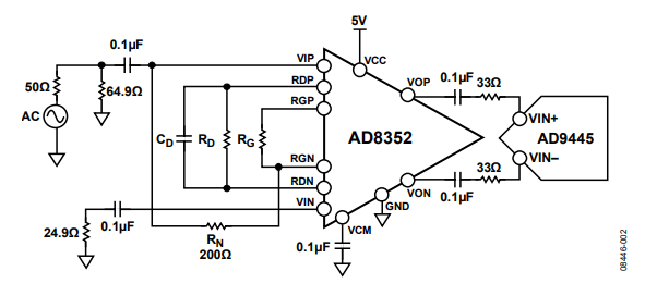
The circuits shown in Figure 1 and Figure 2 provide both a single-ended and a differential configuration for driving high-speed analog-to-digital converters (ADCs) using the AD8352 ultralow distortion differential radio frequency/intermediate frequency (RF/IF) amplifier. The AD8352 provides the gain, isolation, and distortion performance necessary for efficiently driving high linearity converters, such as the AD9445. The AD8352 also provides balanced outputs whether driven differentially or single-ended, thereby maintaining excellent second-order distortion levels.
Circuit Description
Figure 1 and Figure 2 show two front-end circuits for driving the AD9445 14-bit ADC at 105 MSPS. Figure 1 shows a differential input configuration, and Figure 2 shows a single-ended input configuration.

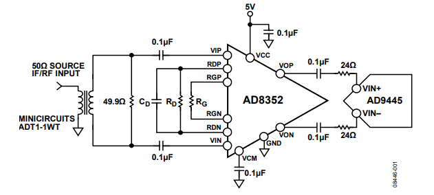

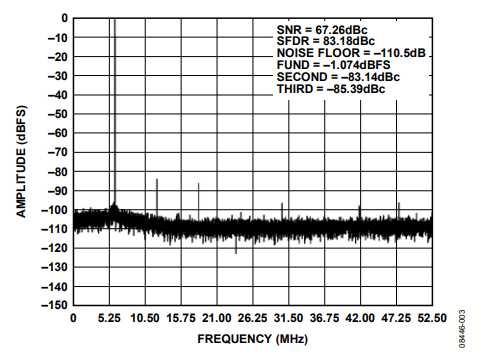
In the differential configuration shown in Figure 1, the input 49.9 Ω resistor provides a differential input impedance to the 50 Ω RF/IF source. When the driver is located less than approximately one eighth of the wavelength of the maximum input RF/IF frequency from the AD8352, impedance matching is not required, thereby eliminating the need for this termination resistor. The output 24 Ω series resistors provide isolation from the input capacitance of the ADC, and the optimum value is determined empirically. The 100 MHz fast Fourier transform (FFT) plots shown in Figure 3 and Figure 4 display the performance results for the differential configuration.


In the single-ended input configuration shown in Figure 2, the net input impedance at VIP is RN (200 Ω) plus the external 24.9 Ω balancing resistor, or approximately 225 Ω. This input requires a 64.9 Ω parallel resistor to provide the input impedance match for a 50 Ω source. If input reflections are minimal, this impedance match is not required. The 200 Ω resistor (RN) is required to balance the output voltages to minimize second-order distortion.
The single-ended configuration provides −3 dB bandwidths similar to input differential drive and shows little or no degradation in overall third-order harmonic performance. The single-ended, third-order distortion levels are similar to the differential FFT plots in Figure 3 and Figure 4. The single-ended circuit avoids the use of a transformer or balun in front of the amplifier while still maintaining excellent distortion up to approximately 100 MHz. However, at frequencies above approximately 100 MHz, second-order distortion increases when the AD8352 is driven single-ended due to phase-related errors.
In both configurations, RG is the gain setting resistor for the AD8352, with the RD and CD components providing distortion cancellation. The AD9445 differential input impedance is approximately 2 kΩ in parallel with 5 pF and requires a 2.0 V p-p differential signal (VREF = 1 V) between VIN+ and VIN− for a fullscale input signal.
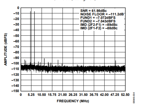
The output of the amplifier is ac-coupled to allow an optimum common-mode voltage at the ADC input. The common-mode voltage at the input of the AD9445 is set to 3.5 V by an internal network. Input ac-coupling can be required if the source also requires a common-mode voltage that is outside the optimum range of the AD8352. A VCM common-mode pin is provided on the AD8352 that equally shifts both input and output common-mode levels. Increasing the gain of the AD8352 increases the system noise and, thus, decreases the signal-to-noise ratio (SNR) (3.5 dB at 100 MHz input for AV = 10 dB) of the AD9445 when no filtering is used. However, note that amplifier gains from 3 dB to 18 dB, with proper selection of CD and RD, do not appreciably affect distortion levels. These circuits, when configured properly, can result in spurious-free dynamic range (SFDR) performance of better than 87 dBc at 70 MHz and 82 dBc at 180 MHz input. Single-ended drive, with appropriate CD and RD, gives similar results for SFDR and third-order intermodulation levels, as shown in Figure 3 and Figure 4.
Excellent layout, grounding, and decoupling techniques must be used to achieve the desired performance from the circuits discussed in this application note. As a minimum, it is recommended to use a 4-layer printed circuit board (PCB) with one ground plane layer, one power plane layer, and two signal layers.
All IC power pins must be decoupled to the ground plane with low inductance multilayer ceramic capacitors (MLCCs) of 0.01 µF to 0.1 µF (these capacitors are not shown in Figure 1 and Figure 2, for simplicity). Follow the recommendations on the individual data sheets for the ICs.
The product evaluation board user guides must be consulted for recommended layout and critical component placement. The user guides can be accessed through the main product pages for the devices or their data sheets.
Common Variations
Placing antialiasing filters between the ADC and the amplifier is a common approach for improving overall noise and broadband distortion performance for both band-pass and low-pass applications. For high-frequency filtering, matching to the filter is required. The AD8352 maintains a 100 Ω output impedance well beyond most applications and is well suited to drive most filter configurations with little or no degradation in distortion.
The AD8352 low distortion differential amplifier can be replaced by the high third-order intercept (IP3), low noise figure AD8375 variable gain amplifier (VGA). The AD8375 is a digitally controlled, variable gain, wide bandwidth amplifier that provides precise gain control across a broad 24 dB gain range, with 1 dB resolution. The AD8376 is a dual version of the AD8375. (See the AN-1408 Application Note, Using the AD8376 VGA to Drive Wide Bandwidth ADCs for High IF AC-Coupled Applications.)
References
MT-031 Tutorial, Grounding Data Converters and Solving the Mystery of AGND and DGND. Analog Devices.
MT-073 Tutorial, High Speed Variable Gain Amplifiers (VGAs). Analog Devices.
MT-075 Tutorial, Differential Drivers for High Speed ADCs Overview. Analog Devices.