AN-1499: AD7266 SAR ADC in DC-Coupled Differential and Single-Ended Applications
Circuit Function and Benefits
The driver circuits shown in this circuit note are optimized for dc-coupled applications requiring low distortion and low noise performance. This drive circuit ensures that the maximum AD7266 performance is achieved by providing adequate settling time, low distortion, and low output impedance.
Circuit Description
In applications where the signal source has high impedance, it is recommended to buffer the analog input signal before applying it to the switched capacitor inputs of the AD7266. This buffer isolates the source from the transient currents that appear at the input of the analog-to-digital converter (ADC). A dual op amp pair can be used to directly couple a differential signal to one of the analog input pairs of the AD7266. The AD8022 is an ideal choice for the dual op amp and has low power (4.0 mA per amplifier), low noise (2.5 nV/√Hz at 100 kHz), and low distortion (110 dB spurious-free dynamic range (SFDR) at 200 kHz). The AD7266 has a specified minimum acquisition time of 90 ns with a supply voltage of 5 V. This acquisition time is the time from when the device enters track mode until the next conversion is initiated. The op amp selected must have adequate settling time to meet the acquisition time requirements of the AD7266 and achieve the specified performance.
The circuit configuration shown in Figure 1 shows how an AD8022 op amp can convert a bipolar single-ended signal into a unipolar differential signal that can be applied directly to the AD7266 analog inputs. The circuit not only performs the single-ended to differential conversion but also level shifts the output signal to match the ADC input range. The voltage applied to Point A in Figure 1 sets up the common-mode voltage for each half of the AD8022. The 10 kΩ/20 kΩ divider generates this voltage (1.67 V) from the AD7266 2.5 V internal reference. If using the on-chip 2.5 V reference on the AD7266 elsewhere in a system (as shown in Figure 1 and Figure 2), the output from DCAPA and DCAPB must first be buffered. Use the OP177, which features a high precision performance, as a reference buffer.

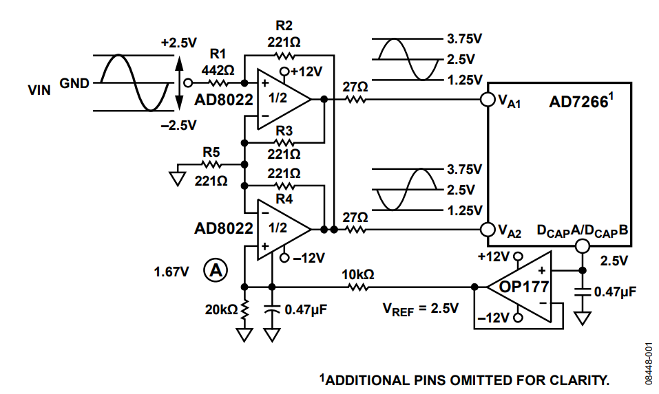
(Simplified Schematic; Decoupling and All Connections Not Shown)
The primary negative feedback path is provided by Resistor R2 to Resistor R1, and the gain from VIN to VA2 is set by the ratio of Resistor R2 to Resistor R1. In this case, the ratio is 0.5. The common-mode voltage of 1.67 V at the input of the upper half of the AD8022 produces an output common-mode voltage at VA2 of (1 + R2/R1) × 1.67 V = 2.5 V. Localized feedback supplied by Resistor R3 and Resistor R4 produce a signal at VA1, which is 180° out of phase with the signal at VA2.
When the input voltage is zero, VA1 and VA2 must be 2.5 V. This voltage requires a current in both R3 and R4 of:
(2.5 V - 1.67 V)/221 Ω = 3.76 mA
The current through R5 is, therefore, 2 × 3.76 mA = 7.52 mA. Therefore, R5 must be equal to R3 and R4 to force the common-mode voltage at VA1 to be 2.5 V.
The AD7266 can have a total of 12 single-ended analog input channels. The analog input range can be programmed to be either 0 V to VREF or 0 V to 2 × VREF. Figure 2 shows a typical connection diagram when operating the ADC in single-ended mode, where an AD8022 drives a pair of discrete channels. The AD8021 is a high performance single op amp that can be used as an alternative to a dual device in very high performance systems. The absolute value of R is flexible, but it must be chosen to achieve the desired bandwidth of the op amp.

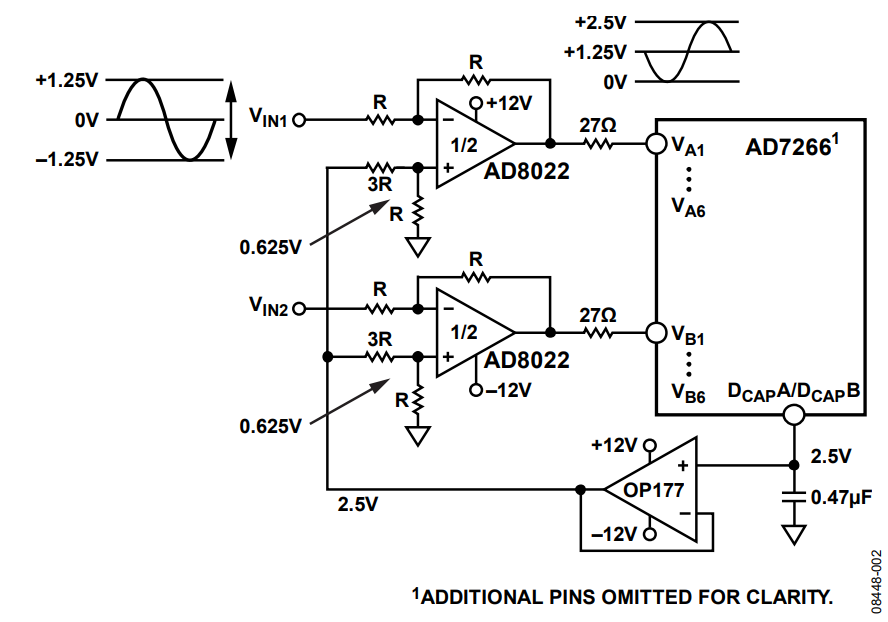
(Simplified Schematic; Decoupling and All Connections Not Shown)
In Figure 1 and Figure 2, the AD8022 operates on dual 12 V supplies, whereas the AD7266 is specified for power supply voltages of 2.7 V to 5.25 V. Ensure the maximum input voltage limits of the AD7266 are not exceeded during transient or power-on conditions (see MT-036 Tutorial). In addition, the circuit must be constructed on a multilayer PC board with a large area ground plane. Proper layout, grounding, and decoupling techniques must be used to achieve optimum performance (see MT-031 Tutorial, MT-101 Tutorial, and the EVAL-AD7266 evaluation board layout).
Common Variations
The OP07D, an ultralow offset voltage op amp, is a lower cost alternative to the OP177. It offers similar performance with the exception of the input offset voltage specification.
References
MT-036 Tutorial, Op Amp Output Phase-Reversal and Input Over-Voltage Protection, Analog Devices.
MT-074 Tutorial, Differential Drivers for Precision ADCs, Analog Devices.
MT-075 Tutorial, Differential Drivers for High Speed ADCs Overview, Analog Devices.
MT-076 Tutorial, Differential Driver Analysis, Analog Devices.