AN-1406: Designing an Inverting Power Supply Using the ADP5300/ADP5301/ ADP5302/ADP5303 Ultralow Power, Step-Down DC-to-DC Regulators
Introduction
Certain applications, such as bipolar amplifier, optical module, and charge-coupled device (CCD) bias, usually require a negative output voltage from a positive input voltage. Designers of power management systems need versatile switching controllers and regulators that allow them to solve these power management challenges. The ADP5300/ADP5301/ADP5302/ADP5303 ultralow power, step-down dc-to-dc regulators from Analog Devices, Inc., provide an ultralow quiescent current, synchronous step-down functionality. These regulators can step down to 0.8 V ranges with an input supply voltage range of 2.15 V to 6.50 V and an output current of up to 500 mA.
Although targeted for synchronous step-down applications, the versatility of the ADP5300/ADP5301/ADP5302/ADP5303 allows these devices to implement an inverting buck-boost topology, which can generate a negative output voltage from a positive input voltage without increasing the cost, the quantity of external components, or the size of the solution.
The ultralow power technology allows the ADP5300/ADP5301/ ADP5302/ADP5303 to achieve high efficiency in light load operation with hysteresis mode. The devices can operate in pulse-width modulation (PWM) mode to achieve low noise performance and heavy load operation.
This application note describes how to implement the ADP5300/ ADP5301/ADP5302/ADP5303 in a synchronous inverting buckboost topology to generate negative output voltages from positive input voltages. This application note also discusses some limitations of the buck-boost topology and the possible solutions.
Buck-Boost Topology Basics
Figure 1 shows a simplified buck-boost topology. The topology consists of an inductor, two power switches operating out of phase from one another, an input capacitor and an output capacitor.

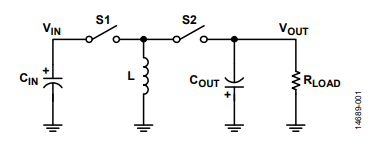
Figure 2 and Figure 3 show the current flow path during the S1 on time and the S1 off time, respectively. During the on time, Switch S1 is on, Switch S2 is off, and the current flows from the input capacitor, charging the inductor while the output capacitor provides energy to the load. During the off time, Switch S1 is off, Switch S2 is on, and the current flows from the inductor to the load while charging the output capacitor.

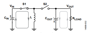

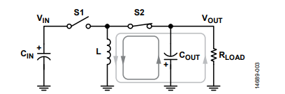
Note that the current flows from ground to VOUT, which results in a negative output voltage.
In Equation 1, the steady state conversion ratio is written by applying the principles of inductor voltage-second balance and the capacitor charge balance to the topology. Equation 2 specifies the dc inductor current value, IL, in PWM mode. Equation 3 details the inductor ripple current, ΔIL.


where:
VOUT is the output voltage.
VIN is the input voltage.
D is the duty cycle:

IOUT is the output current.
L is the inductor.
fSW is the switching frequency.
Implementing the Buck-Boost Topolgy With the ADP5300 to the ADP5303
When using the ADP5300/ADP5301/ADP5302/ADP5303 synchronous buck regulators to implement the buck-boost topology inverting power supply application, consider the design restrictions listed in Table 1.
| Voltage and Current | Restriction | Parameter | Value |
| VIN_MIN | > | VUVLO | 2.06 V |
| VIN_MAX + |VOUT| | < | VMAX | 6.50 V |
| IL_PEAK_HYS | < | ILIM_HYS | 265 mA |
| IL_PEAK_PWM | < | ILIM_PWM | 1000 mA |
The minimum input voltage of the buck-boost circuit must be greater than the UVLO voltage of the ADP5300/ADP5301/ ADP5302/ADP5303, which must typically be 2.06 V for the regulators to work. The sum of the maximum input voltage and the absolute value of the output voltage must be less than the maximum operation input voltage of the regulators, which has a typical value of 6.50 V. For the circuit to work normally, ensure that the peak inductor current is less than the minimum current limit trigger point of the regulator.

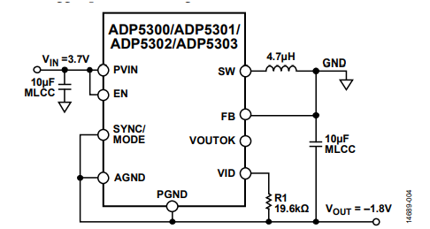
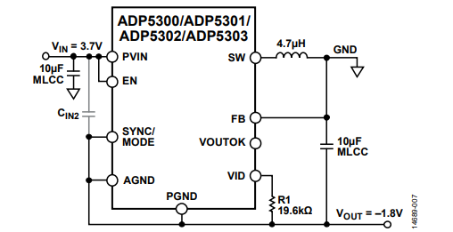
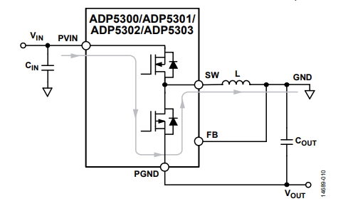
To convert the synchronous buck regulator into the buck-boost topology, connect the inductor and the output capacitor just like in the buck topology. Note that the ground and the output voltage points are reversed (see Figure 4). The output voltage is the same as the buck topology set by an external VID resistor. Refer to Table 2 for the resistor values.
| VID Configuration | VOUT (V) | |
| Factory Option 0 | Factory Option 1 | |
| Short to AGND | −3.0 | −3.1 |
| Short to PVIN | −2.5 | −1.3 |
| RVID = 499 kΩ | −3.6 | Not applicable |
| RVID = 316 kΩ | −3.3 | Not applicable |
| RVID = 226 kΩ | −2.9 | −4.2 |
| RVID = 174 kΩ | −2.8 | −3.9 |
| RVID = 127 kΩ | −2.7 | −3.4 |
| RVID = 97.6 kΩ | −2.6 | −3.2 |
| RVID = 76.8 kΩ | −2.4 | −1.9 |
| RVID = 56.2 kΩ | −2.3 | −1.7 |
| RVID = 43 kΩ | −2.2 | −1.6 |
| RVID = 32.4 kΩ | −2.1 | −1.4 |
| RVID = 25.5 kΩ | −2.0 | −1.1 |
| RVID = 19.6 kΩ | −1.8 | −1.0 |
| RVID = 15 kΩ | −1.5 | −0.9 |
| RVID = 11.8 kΩ | −1.2 | −0.8 |
Inductor Selection
The operating frequency, the input voltage, and the inductor ripple current determine the inductor value. Considering the peak inductor current, employing a larger inductor than the inductor employed in the buck topology is recommended. However, the inductance must not be too large because it affects the loop stability. To avoid a premature current limit, ensure that the peak inductor current does not exceed the minimum peak current-limit threshold (ILIM_PWM in PWM mode and ILIM_HYS in hysteresis mode).
Calculate the peak inductor current by adding the average inductor current and half of the peak-to-peak inductor ripple current.

where:
IAVG is the average inductor current.

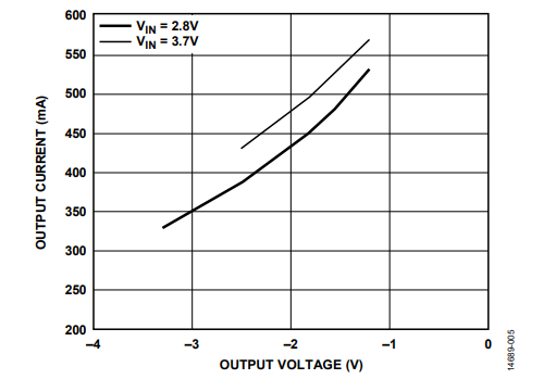
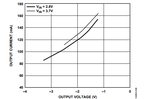
Taking the peak inductor current into account, the load current capability of the ADP5300/ADP5301/ADP5302/ADP5303 in the inverting buck-boost topology for the common input voltages in PWM mode and hysteresis mode is shown in Figure 5 and Figure 6, assuming a 4.7 μH inductor and a 2 MHz switching frequency.


The saturation current of the inductor must be greater than the peak inductor current. For ferrite core inductors with a quick saturation characteristic, the saturation current rating of the inductor must be greater than the current-limit threshold of the switch to prevent the inductor from saturation through normal operation.
Output Capacitor Selection
Note that the output current is discontinuous in the inverting buck-boost topology. The output capacitors supply energy to the load during the on time when energy stored in the inductor increases. During the off time, the inductor delivers energy to both the load and the output capacitors.
A major concern with the capacitance of the output capacitors is the allowable output voltage ripple that is determined by two parameters of the output capacitors. One is the capacitance and the other is the equivalent series resistance (ESR) of the output capacitors. The following equation gives an estimated value of the minimum capacitance (COUT) required to keep the output voltage ripple within the allowable range:

where:
ΔVRIPPLE is the allowable output ripple voltage.
ESR is the total equivalent series resistance of the output capacitors.
IPEAK is the inductor peak current.
To achieve the lowest possible output ripple voltage, multilayer ceramic capacitors (MLCCs) that have very low ESR values are recommended. The rms current rating of the selected output capacitors must be greater than the values calculated using the following equation:

Input Capacitor Selection
The input current is also discontinuous in the inverting buckboost topology. Assuming that the input voltage deviation due to energy depletion of the input capacitor during the power on time is lower than 5% of the input voltage, the following equation calculates the minimum input capacitance (CIN) needed to meet this requirement:

where:
IAVG is the average inductor current.
ESRCIN is the equivalent series resistance of the input capacitors.
At least one piece of a 10 μF ceramic capacitor is recommended and it must be placed as close to the PVIN pin as possible. The rms current of the selected input capacitor must be greater than the value calculated in the following equation:

Although the majority of the capacitance on the input voltage rail is referenced to the system ground, an additional input decoupling capacitor placed from the input voltage to the PGND pin of the ADP5300/ADP5301/ADP5302/ADP5303 can reduce the output voltage ripple and improve the transient response, as shown in Figure 7.

Enable Signal Level Shifting
The ADP5300/ADP5301/ADP5302/ADP5303 has an EN pin to enable and disable the regulator. However, in the inverting buck-boost application, the IC is referenced to the negative output voltage instead of the system ground. If the EN pin is connected to the system ground with the intention of disabling the regulator, the ADP5300/ADP5301/ADP5302/ADP5303 may still be switching.
A possible solution for this enable signal is using an ultralow power inverter, a P-type metal-oxide semiconductor field effect transistor (MOSFET), and a resistor with the proper connection to form an EN level shifting circuit as shown in Figure 8.

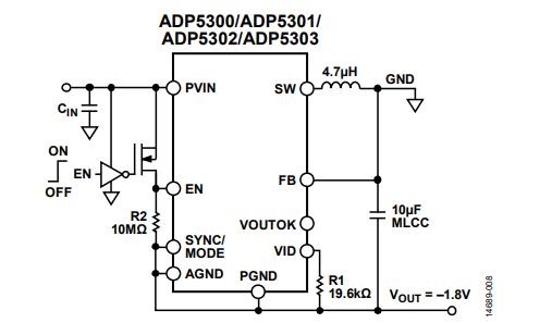
Note that the precision enable feature of the ADP5300/ ADP5301/ADP5302/ADP5303 is lost when the level shifting circuit is used. If the enable function is not needed, simply connect the EN pin to the input voltage as shown in Figure 8.
Reduce VOUT Ramp Up Before Startup
When using a synchronous buck regulator to achieve the inverting buck-boost topology, one common issue is that the output voltage can ramp up and become a positive voltage before the regulator starts to work (see Figure 9).

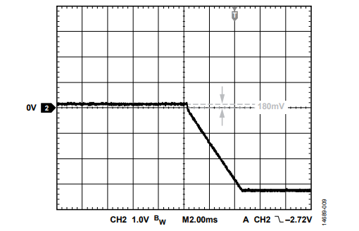
This positive output voltage ramping up is caused by the shutdown current of the regulator flowing from the PGND pin of the IC through the body diode of the low-side MOSFET and back to the system ground, as shown in Figure 10. The body diode of the low-side MOSFET clamps VOUT at the forward voltage level with a typical value of approximately 180 mV, because the ADP5300/ ADP5301/ADP5302/ADP5303 shutdown current is very small.

As VOUT is connected to the PGND pin of the regulator, which is actually the reference point for the internal circuits such as UVLO, the positive voltage shown in the PGND pin reduces the UVLO threshold voltage. The regulator can fail to start up when the input voltage is very close to the UVLO threshold voltage of the regulator, which has a typical value of 2.06 V
This issue is observable in nearly all synchronous buck regulators when they are used to perform the inverting buckboost topology described in this application note. It is very difficult to eliminate the issue entirely.
Conclusion
Implementing the ADP5300/ADP5301/ADP5302/ADP5303 in the inverting buck-boost topology can be as simple, inexpensive, and small in solution size as the buck implementation. This application note provides a simple EN level shifting circuit when the enable/ disable functionality is needed and describes an issue with the VOUT ramping up to a positive voltage when applying the synchronous buck regulator into the inverting buck-boost topology.
By following the design equations and suggestions in this application note, a system designer can ensure a robust design that satisfies all requirements.
Authors
