This application note explains several aspects of the digital filtering associated with the Σ-Δ modulators used in the ADE7912/ ADE7913. The role of the filters is to decimate the outputs of the modulators to various rates, while eliminating high frequency noise. These rates start from a high of 8 kHz and go as low as 1 kHz, allowing the user to update the rates to the microcontroller processing bandwidth.
Digital Decimation Filtering
Functional Description
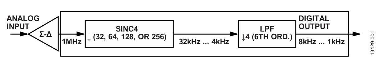
Figure 1 shows the block diagram of the decimation filtering implemented in the ADE7912/ADE7913. The Σ-Δ modulator provides a bit stream with a frequency of 1 MHz when the chip is clocked at CLKIN = 4.096 MHz. The SINC4 filter uses four decimation ratios—32, 64, 128, and 256—to provide outputs at 32 kHz, 16 kHz, 8 kHz and 4 kHz. To limit the bandwidth to meaningful frequencies while also keeping the data rate as low as possible, an extra low-pass filter (LPF) with 60 dB attenuation is used. This makes the subsequent rms and power calculations more precise, reducing the bandwidth a micro-controller must reserve for the metrology calculations.
Figure 1. Block diagram of the decimation filtering implemented in the ADE7912/ADE7913.
The LPF performs another decimation by 4, and has internal flexibility, which leads to two different bandwidths. The LPF is implemented as two separate, sixth-order filters: one filter for the narrower bandwidths, one filter for the larger bandwidths.
The ADE7912/ADE7913 provide multiple output data rates (ODRs): 8 kHz, 4 kHz, 2 kHz, and 1 kHz, as well as two selectable bandwidths for each of these rates (see Table 1). The selectable ODRs help users address a wide range of scenarios to make their own trade-offs in the datapaths implemented in the microcontroller.
Table 1. CONFIG Register Settings for Obtaining Various ODRs and Bandwidths
CONFIG Register
ODR (kHz)
SINC4 + LPF Bandwidth (kHz)
Bits[5:4] (ADC_FREQ) Setting
Bit 7 (BW) Setting
00
0
8
3.338
00
1
8
2.137
01
0
4
1.670
01
1
4
1.069
10
0
2
0.836
10
1
2
0.535
11
0
1
0.418
11
1
1
0.268
ODR and bandwidth selection is performed by Bit 7 (BW) and Bits[5:4] (ADC_FREQ) in the CONFIG register. Table 1 shows the different BW and ADC_FREQ settings required when the ADE7912/ADE7913 is clocked at CLKIN = 4.096 MHz. The bandwidth is indicated by the point at which the gain is attenuated by 3 dB.
Frequency Response and Time Delay Characteristics of the SINC4 + LPF Filters
The equivalent Z-domain formula of the SINC4 for various decimation ratios (DRs) is shown in the following equation:
The Z-domain formula of the LPF that corresponds to the narrower bandwidth (BW, Bit 7 of the CONFIG register, is set to 1) is shown in the following equation:
where LPF_BW1 is the LPF that corresponds to the narrower bandwidth.
The Z-domain formula of the LPF that corresponds to the larger bandwidth (BW, Bit 7 of the CONFIG register, is cleared to 0) is shown in the following equation:
where LPF_BW2 is the LPF that corresponds to the larger bandwidth.
Magnitude Frequency Response and Time Delays for Various Filters
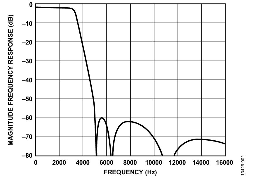
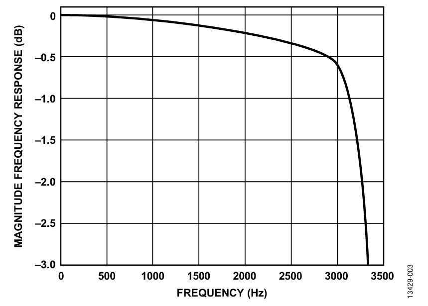
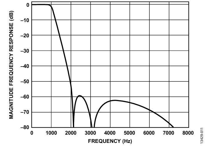
Figure 2 through Figure 25 and Table 2 through Table 32 provide detailed information about the magnitude frequency response and the time delays introduced in the signal path by the various filters. The output data rate (ODR) is the output frequency at which the analog-to-digital converter (ADC) samples are provided by the ADE7912/ADE7913. The bandwidth of the filter (BW) is the point at which the gain is attenuated by 3 dB. The full frequency response, or the response up to the −3 dB point, and the flat-band response (from 0 dB down to −0.8 dB attenuation) are shown in all ODR and BW cases.
The phase delay defines the propagation delay in the phase of a sinusoidal signal passing through the filter. Tables showing the phase delay at various frequencies are shown for all ODR and BW cases.
From the perspective of power calculations, these time delays do not affect the final results because both voltage and current signals are subject to identical time delay propagation. However, in case of transient events or events synchronous to the zero crossings, it may be useful to know the time delays.
The frequency points are selected in such a way that the intermediate values can be obtained with accuracy by piecewise linear interpolation. These frequency points may be useful, for example, if amplitude corrections are necessary.
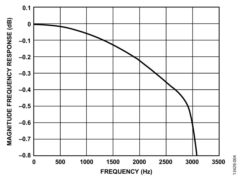
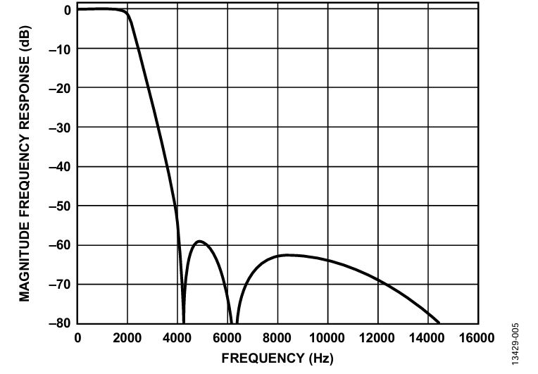
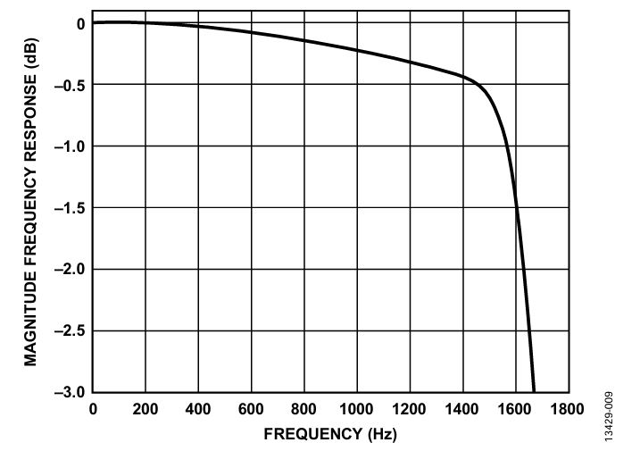
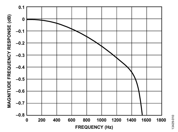
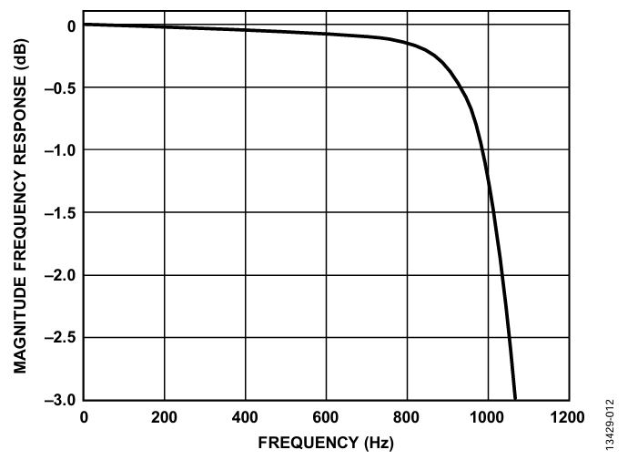
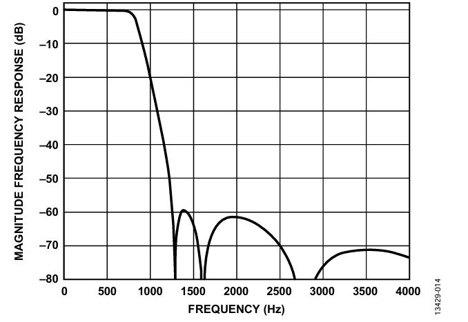
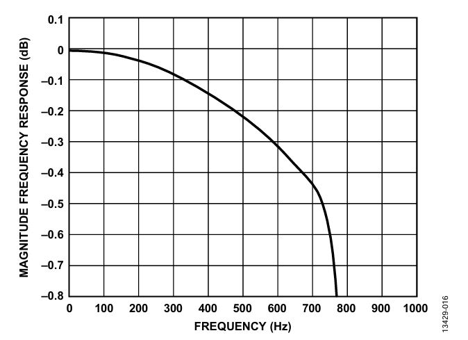
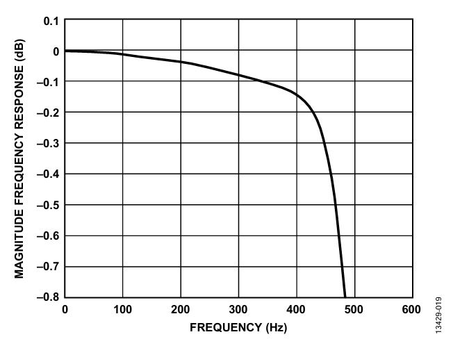
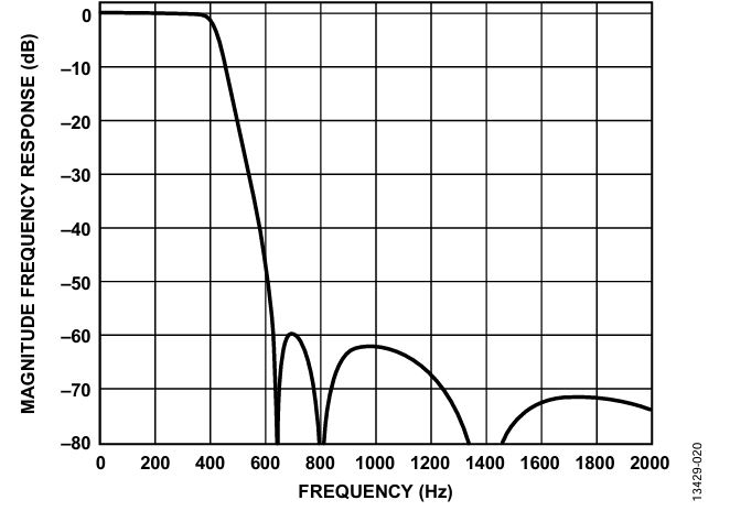
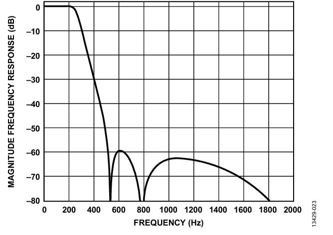
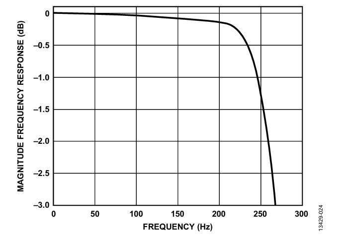
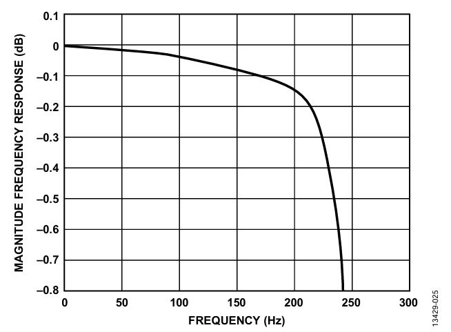
ODR = 8 kHz and BW = 3.338 kHz
Figure 2. Full frequency response for ODR = 8 kHz and BW= 3.338 kHz.
Figure 3. 3 dB point response for ODR = 8 kHz and BW = 3.338 kHz.
Figure 4. Flat-band response for ODR = 8 kHz and BW = 3.338 kHz.
Table 2. SINC4 + LPF Gain Response at Various Frequencies for ODR = 8 kHz and BW = 3.338 kHz; Frequency Range = 50 Hz to 450 Hz
Frequency (Hz)
50
100
150
200
250
300
350
400
450
Magnitude (milli_dB)
0
−0.32
−0.87
−1.66
−2.67
−3.93
−5.44
−7.21
−9.26
Table 3. SINC4 + LPF Gain Response at Various Frequencies for ODR = 8 kHz and BW = 3.338 kHz; Frequency Range = 500 Hz to 900 Hz
Frequency (Hz)
500
550
600
650
700
750
800
850
900
Magnitude (milli_dB)
−11.6
−14.22
−17.15
−20.40
−23.97
−27.87
−32.11
−36.69
−41.61
Table 4. SINC4 + LPF Gain Response at Various Frequencies for ODR = 8 kHz and BW = 3.338 kHz; Frequency Range = 950 Hz to 1350 Hz
Frequency (Hz)
950
1000
1050
1100
1150
1200
1250
1300
1350
Magnitude (milli_dB)
−46.86
−52.45
−58.37
−64.6
−71.13
−77.95
−85.05
−92.41
−100
Table 5. SINC4 + LPF Gain Response at Various Frequencies for ODR = 8 kHz and BW = 3.338 kHz; Frequency Range = 1400 Hz to 2200 Hz
Frequency (Hz)
1400
1500
1600
1700
1800
1900
2000
2100
2200
Magnitude (dB)
−0.108
−0.124
−0.141
−0.159
−0.177
−0.197
−0.218
−0.241
−0.265
Table 6. SINC4 + LPF Gain Response at Various Frequencies for ODR = 8 kHz and BW = 3.338 kHz; Frequency Range = 2300 Hz to 3100 Hz
Frequency (Hz)
2300
2400
2500
2600
2700
2800
2900
3000
3100
Magnitude (dB)
−0.291
−0.318
−0.346
−0.374
−0.402
−0.434
−0.486
−0.6
−0.859
Table 7. SINC4 + LPF Gain Response at Various Frequencies for ODR =8 kHz and BW = 3.338 kHz; Frequency Range = 3200 Hz to 3500 Hz
Frequency (Hz)
3200
3300
3338
3400
3500
Magnitude (dB)
−1.414
−2.452
−3.0
−4.09
−6.27
Table 8. SINC4 +LPF Phase Delay Response at Various Frequencies for ODR = 8 kHz and BW = 3.338 kHz
Frequency (Hz)
50
500
750
1000
1500
2000
2500
3000
3300
Phase Delay (μs)
225
226
227
229
234
241
254
277
321
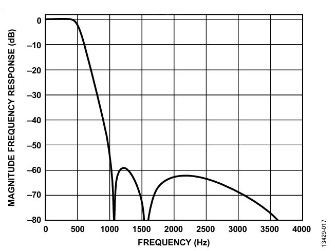
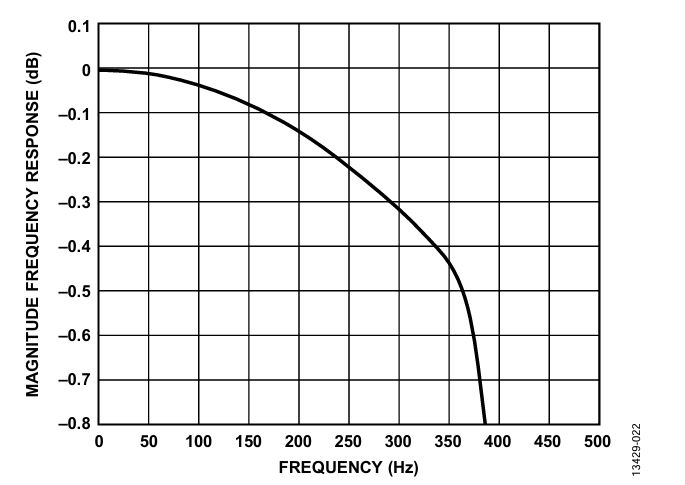
ODR = 8 kHz and BW = 2.137 kHz
Figure 5. Full frequency response for ODR = 8 kHz and BW = 2.137 kHz.
Figure 6. 3 dB Point response for ODR = 8 kHz and BW = 2.137 kHz.
Figure 7. Flat-band response for ODR = 8 kHz and BW = 2.137 kHz.
Table 9. SINC4 + LPF Gain Response at Various Frequencies for ODR = 8 kHz and BW = 2.137 kHz; Frequency Range = 50 Hz to 450 Hz
Frequency (Hz)
50
100
150
200
250
300
350
400
450
Magnitude (milli_dB)
0
−0.56
−1.5
−2.77
−4.34
−6.19
−8.25
−10.51
−12.91
Table 10. SINC4 + LPF Gain Response at Various Frequencies for ODR = 8 kHz and BW = 2.137 kHz; Frequency Range = 500 Hz to 900 Hz
Frequency (Hz)
500
550
600
650
700
750
800
850
900
Magnitude (milli_dB)
−15.44
−18.08
−20.82
−23.68
−26.70
−29.90
−33.36
−37.13
−41.29
Table 11. SINC4 + LPF Gain Response at Various Frequencies for ODR = 8 kHz and BW = 2.137 kHz; Frequency Range = 950 Hz to 1400 Hz
Frequency (Hz)
950
1000
1050
1100
1150
1200
1250
1300
1400
Magnitude (milli_dB)
−45.90
−51.01
−56.64
−62.8
−69.41
−76.40
−83.64
−90.96
−105
Table 12. SINC4 + LPF Gain Response at Various Frequencies for ODR = 8 kHz and BW = 2.137 kHz; Frequency Range = 1500 Hz to 2200 Hz
Frequency (Hz)
1500
1600
1700
1800
1900
2000
2100
2137
2200
Magnitude (dB)
−0.119
−0.140
−0.188
−0.314
−0.621
−1.274
−2.243
−3.01
−4.167
Table 13. SINC4 + LPF Phase Delay Response at Various Frequencies for ODR = 8 kHz and BW = 2.137 kHz
Frequency (Hz)
50
500
750
1000
1500
1750
2000
2100
Phase Delay (μs)
294
296
299
304
322
338
365
377
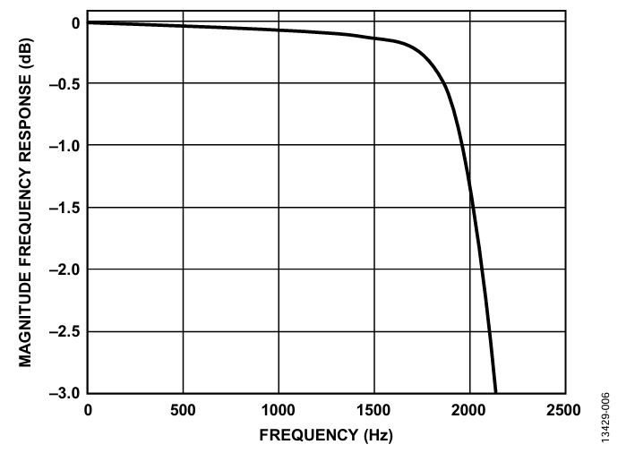
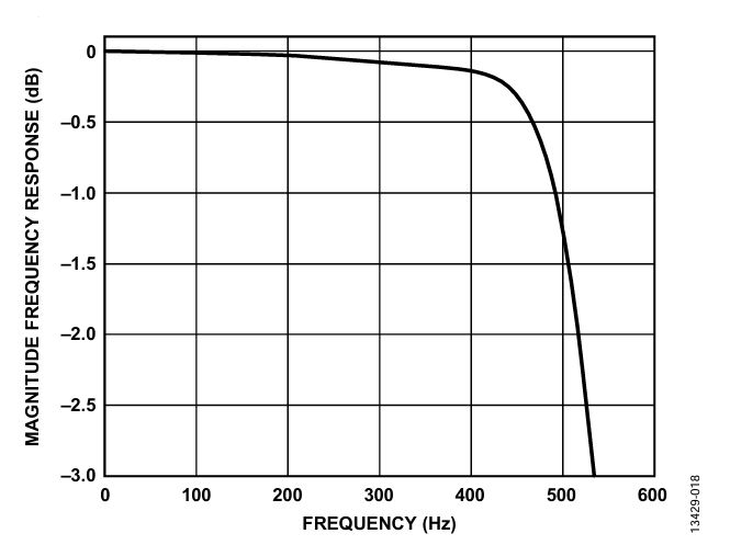
ODR = 4 kHz and BW = 1.67 kHz
Figure 8. Full frequency response for ODR = 4 kHz and BW = 1.67 kHz.
Figure 9. 3 dB Point response for ODR = 4 kHz and BW = 1.67 kHz.
Figure 10. Flat-band response for ODR = 4 kHz and BW = 1.67 kHz.
Table 14. SINC4 + LPF Gain Response at Various Frequencies for ODR = 4 kHz and BW = 1.67 kHz; Frequency Range = 50 Hz to 450 Hz
Frequency (Hz)
50
100
150
200
250
300
350
400
450
Magnitude (milli_dB)
0
−1.323
−3.589
−6.865
−11.234
−16.784
−23.596
−31.732
−41.222
Table 15. SINC4 + LPF Gain Response at Various Frequencies for ODR = 4 kHz and BW = 1.67 kHz; Frequency Range = 500 Hz to 900 Hz
Frequency (Hz)
500
550
600
650
700
750
800
850
900
Magnitude (milli_dB)
−52.06
−64.199
−77.554
−92.011
−107.44
−123.73
−140.81
−158.66
−177.37
Table 16. SINC4 + LPF Gain Response at Various Frequencies for ODR = 4 kHz and BW = 1.67 kHz; Frequency Range = 950 Hz to 1350 Hz
Frequency (Hz)
950
1000
1050
1100
1150
1200
1250
1300
1350
Magnitude (dB)
−0.197
−0.218
−0.240
−0.265
−0.291
−0.318
−0.346
−0.373
−0.401
Table 17. SINC4 + LPF Gain Response at Various Frequencies for ODR = 4 kHz and BW = 1.67 kHz; Frequency Range = 1400 Hz to 1900 Hz
Frequency (Hz)
1400
1450
1500
1550
1600
1670
1700
1800
1900
Magnitude (dB)
−0.433
−0.486
−0.598
−0.856
−1.407
−3.01
−4.071
−8.807
−14.39
Table 18. SINC4 + LPF Phase Delay Response at Various Frequencies for ODR = 4 kHz and BW = 1.67 kHz
Frequency (Hz)
50
250
500
750
1000
1250
1500
1650
Phase Delay (μs)
450
452
458
467
483
508
555
608
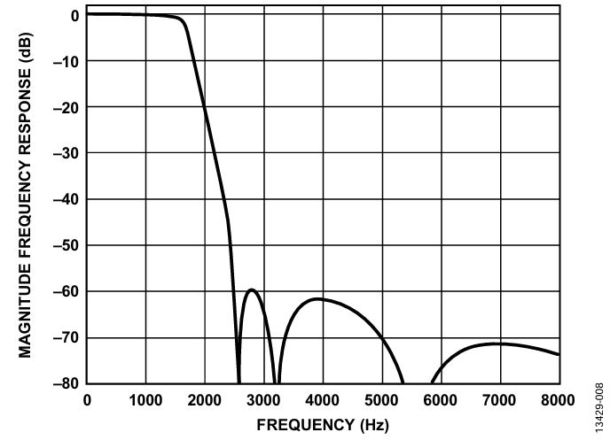
ODR = 4 kHz and BW = 1.069 kHz
Figure 11. Full frequency response for ODR = 4 kHz and BW = 1.069 kHz.
Figure 12. 3 dB Point response for ODR = 4 kHz and BW = 1.069 kHz.
Figure 13. Flat-band response for ODR = 4 kHz and BW = 1.069 kHz.
Table 19. SINC4 + LPF Gain Response at Various Frequencies for ODR = 4 kHz and BW = 1.069 kHz; Frequency Range = 50 Hz to 450 Hz
Frequency (Hz)
50
100
150
200
250
300
350
400
450
Magnitude (milli_dB)
0
−2.19
−5.60
−9.92
−14.85
−20.23
−26.10
−32.76
−40.68
Table 20. SINC4 + LPF Gain Response at Various Frequencies for ODR = 4 kHz and BW = 1.069 kHz; Frequency Range = 500 Hz to 900 Hz
Frequency (Hz)
500
550
600
650
700
750
800
850
900
Magnitude (milli_dB)
−50.39
−62.16
−75.77
−90.33
−104.7
−119.2
−139.8
−186.9
−311.5
Table 21. SINC4 + LPF Gain Response at Various Frequencies for ODR = 4 kHz and BW = 1.069 kHz; Frequency Range = 950 Hz to 1300 Hz
Frequency (Hz)
950
1000
1050
1069
1100
1150
1200
1250
1300
Magnitude (dB)
−0.617
−1.265
−2.423
−3.015
−4.147
−6.326
−8.776
−11.343
−13.936
Table 22. SINC4 + LPF Phase Delay Response at Various Frequencies for ODR = 4 kHz and BW = 1.069 kHz
Frequency (Hz)
50
250
500
750
1000
1250
Phase Delay (μs)
588
593
609
643
730
795
ODR = 2 kHz and BW = 0.836 kHz
Figure 14. Full frequency response for ODR = 2 kHz and BW = 0.836 kHz.
Figure 15. 3 dB Point response for ODR = 2 kHz and BW = 0.836 kHz.
Figure 16. Flat-band response for ODR = 2 kHz and BW = 0.836 kHz.
Table 23. SINC4 + LPF Gain Response at Various Frequencies for ODR = 2 kHz and BW = 0.836 kHz; Frequency Range = 50 Hz to 450 Hz
Frequency (Hz)
50
100
150
200
250
300
350
400
450
Magnitude (milli_dB)
0
−5.5
−15.37
−30.27
−50.55
−76
−106
−139
−176
Table 24. SINC4 + LPF Gain Response at Various Frequencies for ODR = 2 kHz and BW = 0.836 kHz; Frequency Range = 500 Hz to 1000 Hz
Frequency (Hz)
500
550
600
650
700
750
800
836
850
900
950
1000
Magnitude (dB)
−0.216
−0.263
−0.316
−0.372
−0.431
−0.594
−1.39
−3.05
−4.03
−8.75
−14.33
−20.0
Table 25. SINC4 + LPF Phase Delay Response at Various Frequencies for ODR = 2 kHz and BW = 0.836 kHz
Frequency (Hz)
50
125
250
350
400
500
750
830
Phase Delay (μs)
901
904
915
930
939
965
1109
1223
ODR = 2 kHz and BW = 0.535 kHz
Figure 17. Full frequency response for ODR = 2 kHz and BW = 0.535 kHz.
Figure 18. 3 dB Point response for ODR = 2 kHz and BW = 0.535 kHz.
Figure 19. Flat-band response for ODR = 2 kHz and BW = 0.535 kHz.
Table 26. SINC4 + LPF Gain Response at Various Frequencies for ODR = 2 kHz and BW = 0.535 kHz; Frequency Range = 50 Hz to 450 Hz
Frequency (Hz)
50
100
150
200
250
300
350
400
450
Magnitude (milli_dB)
0
−7.69
−17.99
−30.48
−48.05
−73.36
−102.34
−137.17
−305.62
Table 27. SINC4 + LPF Gain Response at Various Frequencies for ODR = 2 kHz and BW = 0.535 kHz; Frequency Range = 500 Hz to 750 Hz
Frequency (Hz)
500
535
550
600
650
700
750
Magnitude (dB)
−1.24
−3.01
−4.10
−8.72
−13.88
−19.01
−24.03
Table 28. SINC4 + LPF Phase Delay Response at Various Frequencies for ODR = 2 kHz and BW = 0.535 kHz
Frequency (Hz)
50
125
250
350
400
500
535
Phase Delay (μs)
1177
1185
1217
1268
1309
1459
1525
ODR = 1 kHz and BW = 0.418 kHz
Figure 20. Full frequency response for ODR = 1 kHz and BW = 0.418 kHz.
Figure 21. 3 dB Point response for ODR = 1 kHz and BW = 0.418 kHz.
Figure 22. Flat-band response for ODR = 1 kHz and BW = 0.418 kHz.
Table 29. SINC4 + LPF Gain Response at Various Frequencies for ODR = 1 kHz and BW = 0.418 kHz; Frequency Range = 50 Hz to 600 Hz
Frequency (Hz)
50
100
150
200
250
300
350
400
418
450
500
550
600
Magnitude (dB)
0
−0.024
−0.070
−0.133
−0.210
−0.310
−0.424
−1.355
−2.98
−8.64
−19.95
−31.74
−45.78
Table 30. SINC4 + LPF Phase Delay Response at Various Frequencies for ODR = 1 kHz and BW = 0.418 kHz
Frequency (Hz)
50
100
150
200
250
300
350
400
Phase Delay (μs)
1806
1820
1843
1879
1930
2005
2122
2349
ODR = 1 kHz and BW = 0.268 kHz
Figure 23. Full frequency response for ODR = 1 kHz and BW = 0.268 kHz.
Figure 24. 3 dB Point response for ODR = 1 kHz and BW = 0.268 kHz.
Figure 25. Flat-band response for ODR = 1 kHz and BW = 0.268 kHz.
Table 31. SINC4 + LPF Gain Response at Various Frequencies for ODR = 1 kHz and BW = 0.268 kHz; Frequency Range = 50 Hz to 400 Hz
Frequency (Hz)
50
100
150
200
250
268
300
350
400
Magnitude (dB)
0
−0.022
−0.065
−0.128
−1.20
−3.0
−8.615
−18.9
−28.91
Table 32. SINC4 + LPF Phase Delay Response at Various Frequencies for ODR = 1 kHz and BW = 0.268 kHz