AN-1368: Ferrite Bead Demystified
Introduction
High resolution, high performance converters and radio frequency (RF) systems require a low noise design of the power supply to achieve optimum performance. Good filtering of power supply noise and high frequency crosstalk reduction between analog and digital domains is required, especially on mixed-signal converters and transceivers.
Power supply noise is more evident with switching regulators, which generate undesired output artifacts that can be harmful to any noise sensitive system. However, due to their high power conversion efficiency, switching regulators are often found in portable devices where prolonged battery life is needed and in systems where thermal limitations exist.
Similar digital and analog voltage rails of mixed-signal ICs are often powered from different power domains. This approach helps to prevent fast digital switching noise coupling onto the sensitive analog supply rail and degrading the converter performance, but it increases system level complexity and cost. With proper high frequency isolation of supply domains, power supplies can be shared between analog and digital domains, simplifying the design and reducing the cost.
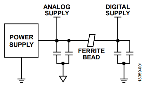
An effective method for filtering high frequency power supply noise and cleanly sharing similar supply rails is the use of ferrite beads. A ferrite bead is a passive device that filters high frequency noise energy over a broad frequency range. It becomes resistive over its intended frequency range and dissipates the noise energy in the form of heat. The ferrite bead is connected in series with the power supply rail and is often combined with capacitors to ground on either side of the bead. This forms a low-pass filter network, further reducing the high frequency power supply noise.
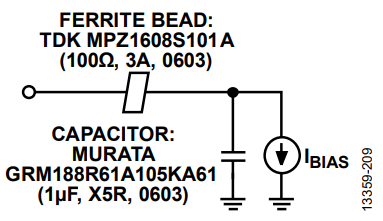
Figure 1 shows an example of a filtering scheme often used in mixed-signal ICs to separate analog and digital supplies. The scheme is suitable for any power distribution network; however, understanding its effectiveness and limitations helps users to avoid characteristics that may, for example, be detrimental in high performance converter applications.

This application note discusses the important considerations that system designers need to be aware of when using ferrite beads in power supply systems, including response characteristics of the ferrite bead, a simplified ferrite bead model and simulation, dc current considerations, LC resonance effects, and damping methods. An understanding of these elements can make the system design approach fast and effective.
The Analog Devices, Inc., products used to demonstrate the effects of ferrite beads as output filters are the 1.25 A, 1.2 MHz synchronous step-down switching regulator (ADP2120) and the 2 A/1.2 A dc-to-dc switching regulator with independent positive and negative outputs (ADP5071).
Ferrite Bead Response Characteristics
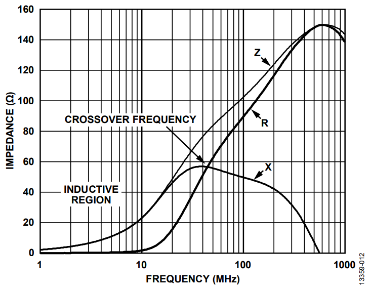
Ferrite beads are categorized by three response regions: inductive, resistive, and capacitive. These regions can be determined by looking at a ZRX plot, where Z is the impedance, R is the resistance, and X is the reactance of the bead. To reduce high frequency noise, the bead must be in the resistive region; this is especially desirable for electromagnetic interference (EMI) filtering applications. The component acts like a resistor, which impedes the high frequency noise and dissipates it as heat. The resistive region occurs after the bead crossover frequency (X = R) and up to the point (shown in Figure 2) where the bead becomes capacitive. This capacitive point occurs at the frequency where the absolute value of capacitive reactance is equivalent to R.

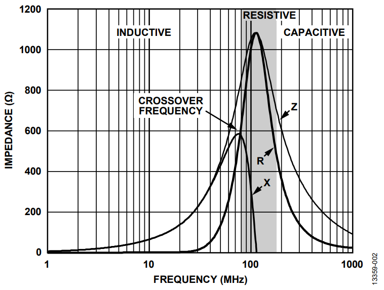
At relatively low frequencies below crossover, the bead response is inductive. At high frequencies, the bead response is capacitive. In this case, the falling slope of the impedance vs. frequency plot is defined by the parasitic capacitance associated with the component.
Ferrite Bead Simplified Model and Simulation
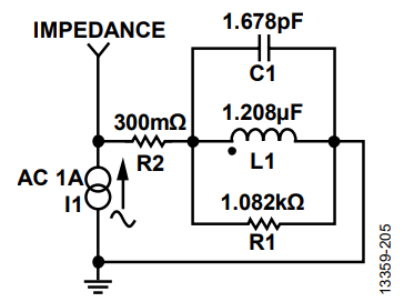
A ferrite bead can be modeled as a simplified circuit consisting of resistors, an inductor, and a capacitor, as shown in Figure 3. RDC corresponds to the dc resistance of the bead. CPAR, LBEAD, and RAC are the parasitic capacitance, the bead inductance, and the ac resistance (ac core losses) associated with the bead.

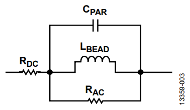
In some cases, the simplified circuit model shown in Figure 3 can be used to approximate the ferrite bead impedance characteristic up to the sub-GHz range.
The Tyco Electronics BMB2A1000LN2 multilayer ferrite bead is used as an example. Figure 4 shows the measured ZRX response of the BMB2A1000LN2 for a zero dc bias current using an impedance analyzer. The circuit simulator suite used was the ADIsimPE, a simulation tool optimized for the design and development of analog and mixed-signal circuits. ADIsimPE is powered by SIMetrix/SIMPLIS.

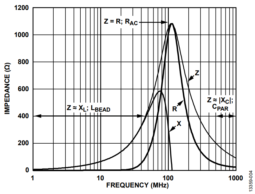
For the region on the measured ZRX plot where the bead appears most inductive (Z ≈ XL; LBEAD), the bead inductance is calculated by the following equation:
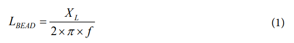
where:
f is the frequency point anywhere in the region the bead appears inductive. In this example, f = 30.7 MHz.
XL is the reactance at 30.7 MHz, which is 233 Ω.
Equation 1 yields an inductance value (LBEAD) of 1.208 μH.
For the region where the bead appears most capacitive (Z ≈ |XC|; CPAR), the parasitic capacitance is calculated by the following equation:
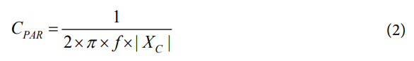
where:
f is the frequency point anywhere in the region the bead appears capacitive. In this example, f = 803 MHz.
|XC| is the reactance at 803 MHz, which is 118.1 Ω.
Equation 2 yields a parasitic capacitance value (CPAR) of 1.678 pF.
The dc resistance (RDC), which is 300 mΩ, is acquired from the manufacturer data sheet. The ac resistance (RAC) is the peak impedance where the bead appears to be purely resistive. Calculate RAC by subtracting RDC from Z. Because RDC is very small compared to the peak impedance, it can be neglected. Therefore, in this case RAC is 1.082 kΩ. The ADIsimPE circuit simulator tool was used to generate the impedance vs. the frequency response. Figure 5 shows both the actual measurement and simulated measurement for the impedance vs. the frequency response at zero dc bias current and Figure 6 shows the circuit simulation model with the calculated values. In this example, the impedance curve from the circuit simulation model closely matches the measured one.

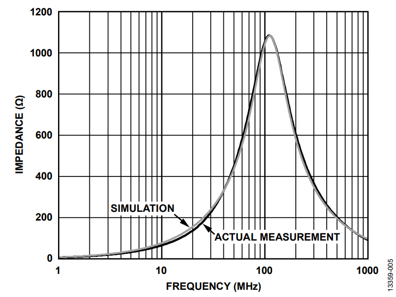

The ferrite bead model can be useful in noise filtering circuit design and analysis. For example, approximating the inductance of the bead can be helpful in determining the resonant frequency cut-off when combined with a decoupling capacitor in a low-pass filter network. However, the circuit model specified in this application note is an approximation with a zero dc bias current. This model may change with respect to dc bias current, and in other cases, a more complex model is required.
DC Bias Current Considerations
Selecting the right ferrite bead for power applications requires careful consideration not only of the filter bandwidth, but also of the impedance characteristics of the bead with respect to dc bias current. In most cases, manufacturers only specify the impedance of the bead at 100 MHz and publish data sheets with frequency response curves at zero dc bias current, similar to those shown in Figure 2. However, when using ferrite beads for power supply filtering, the load current going through the bead is never zero, and as dc bias current increases from zero, all of these parameters change significantly.
As the dc bias current increases, the core material begins to saturate, which significantly reduces the inductance of the ferrite bead. The degree of inductance saturation differs depending on the material used for the core of the component. Figure 7 shows the typical dc bias dependency of the inductance for two ferrite beads. With 50% of the rated currents, the inductance decreases by up to 90%.

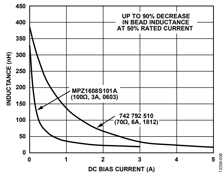
For effective power supply noise filtering, use ferrite beads at about 20% of their rated dc current. As shown in these two examples, the inductance at 20% of the rated current drops to about 30% for the 6 A bead and to about 15% for the 3 A bead. The current rating of ferrite beads is an indication of the maximum current the device can take for a specified temperature rise and not a real operating point for filtering purposes.
In addition, the effect of dc bias current can be observed in the reduction of impedance values over frequency, which in turn reduces the effectiveness of the ferrite bead and its ability to remove EMI. Figure 8 and Figure 9 show how the impedance of the ferrite bead varies with dc bias current.

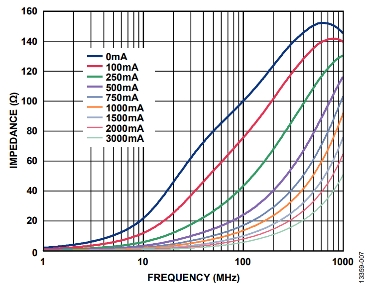

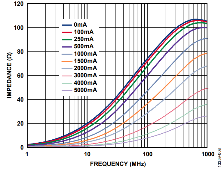
As shown in Figure 8 and Figure 9, the effective impedance at 100 MHz dramatically drops from 100 Ω to 10 Ω for the TDK MPZ1608S101A (100 Ω, 3 A, 0603) and from 70 Ω to 15 Ω for the Wurth Elektronik 742 792 510 (70 Ω, 6 A, 1812) by applying just 50% of the rated current.
System designers must be fully aware of the effect of dc bias current on bead inductance and effective impedance, as this can be critical in applications that demand high supply current. Figure 10 shows the measured attenuation for a 100 Ω, 3 A rated ferrite bead plus a 1 μF capacitor in various dc bias currents, and Figure 11 shows the test circuit model.

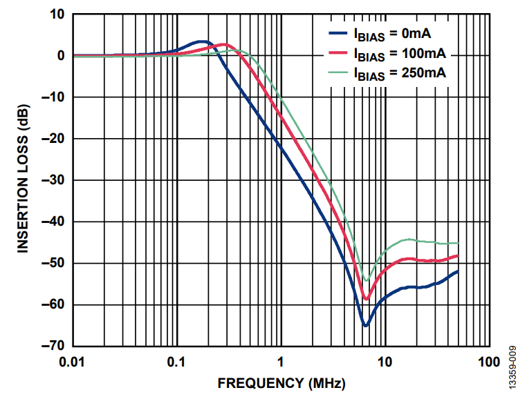

For a 3 A bead with 250 mA of bias current, the resonance cutoff moves to the right mainly due to the inductance drop described in Figure 7.
In addition, the effective attenuation of the network reduces by as much as 15 dB at 1 MHz, where most modern switching regulators operate. This reduction can cause problems if the system engineer relies solely on the data sheet, which shows the impedance at zero dc bias current only. Therefore, to validate the effectiveness of the ferrite bead filter and for accurate results, model the inductance over a range of dc bias current and identify its impedance characteristics under the actual operating conditions.

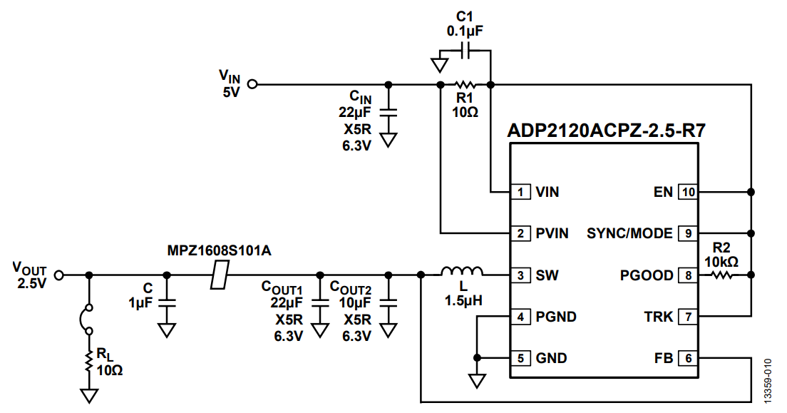
Figure 12 shows an application circuit that uses the ADP2120 buck regulator running in forced pulse-width modulation (FPWM) mode with the ferrite bead filter of Figure 11. With the ADP2120 in FPWM mode, the switching noise spectral output does not change significantly with respect to load current. For more details about FPWM mode, see the ADP2120 data sheet. The spectral output is plotted in Figure 13, showing the effects of dc bias on ferrite bead response.

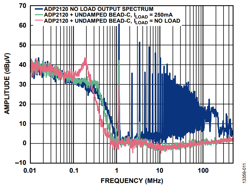
As the load current increases in Figure 13, the filter cutoff frequency moves to the right from approximately 180 kHz with no load to approximately 370 kHz with 250 mA (red trace vs. green trace). The fundamental ripple at around 1.2 MHz attenuates by 30 dB with no load but reduces to about 18 dB with a load of 250 mA.
LC Resonance Effect
Resonance peaking is possible when implementing a ferrite bead together with a decoupling capacitor. This commonly overlooked effect can be detrimental because it may amplify ripple and noise in a given system instead of attenuating it. In many cases, this peaking occurs around popular switching frequencies of dc-to-dc converters.
Peaking occurs when the resonant frequency of a low-pass filter network, formed by the ferrite bead inductance and the high Q decoupling capacitance, is below the crossover frequency of the bead. The resulting filter is underdamped. Figure 14 shows the measured impedance vs. frequency plot of the TDK MPZ1608S101A. The resistive component, which is depended upon to dissipate unwanted energy, does not become significant until about 20 MHz to 30 MHz. Below this frequency, the ferrite bead still has a very high Q and acts like an ideal inductor. LC resonant frequencies for typical bead filters are generally in the 0.1 MHz to 10 MHz range. For typical switching frequencies in the 300 kHz to 5 MHz range, additional damping is required to reduce the filter Q.

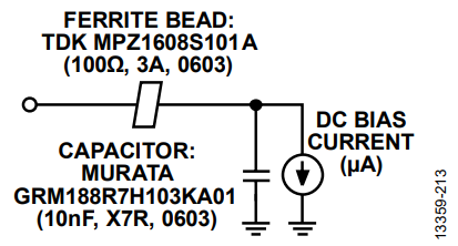
As an example of this effect, Figure 15 shows the S21 frequency response of the bead and capacitor low-pass filter, which displays a peaking effect. The ferrite bead used is a TDK MPZ1608S101A (100 Ω. 3 A, 0603) and the decoupling capacitor used is a Murata GRM188R71H103KA01 low ESR ceramic capacitor (10 nF , X7R, 0603). Load current is in the microampere range.


An undamped ferrite bead filter can exhibit peaks from approximately 10 dB to approximately 15 dB depending on the Q of the filter circuit. In Figure 15, peaking occurs at around 2.5 MHz with as much as 10 dB gain.
In addition, signal gain can be seen from 1 MHz to 3.5 MHz. This peaking is problematic if it occurs in the frequency band in which the switching regulator operates. This amplifies the unwanted switching artifacts, which can wreak havoc on the performance of sensitive loads such as the phased-lock loop (PLL), voltage-controlled oscillator (VCO), and high resolution analog-to-digital converter (ADC). The result shown in Figure 15 has been taken with a very light load (in the microampere range), but this is a realistic application in sections of circuits that need just a few microamperes to 1 mA of load current or sections that are turned off to save power in some operating modes. This potential peaking creates additional noise in the system that can create unwanted crosstalk.
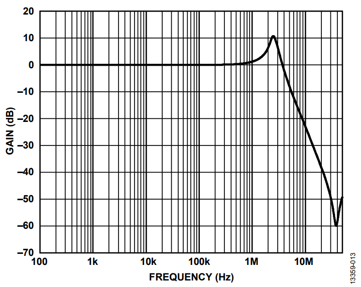
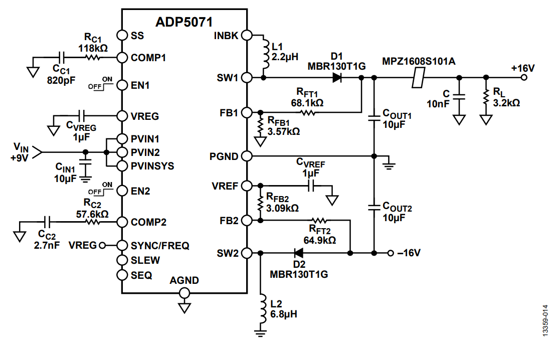
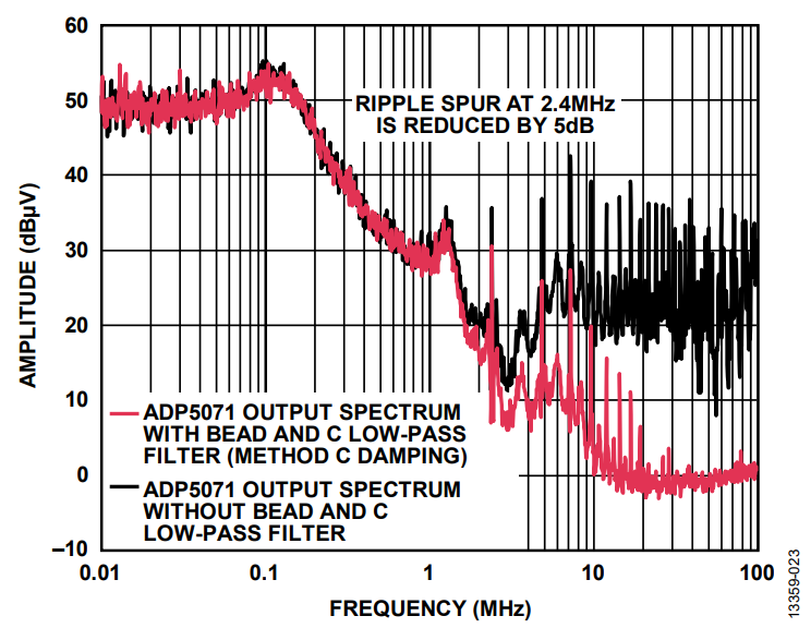
As an example, Figure 17 shows an ADP5071 application circuit with an implemented bead filter and Figure 18 shows the spectral plot at the positive output. The switching frequency is set at 2.4 MHz, the input voltage is set at 9 V, the output voltage is set at 16 V, and the load current is set at 5 mA.


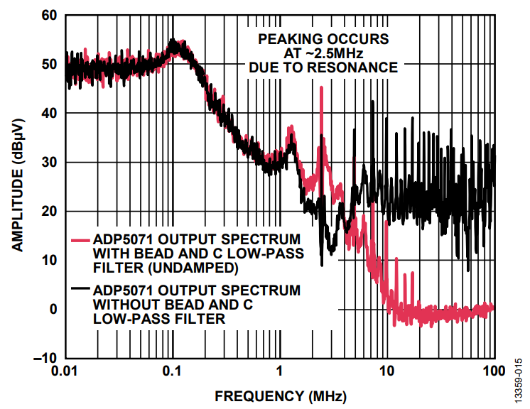
Resonant peaking occurs at around 2.4 MHz due to the inductance of the bead and the 10 nF ceramic capacitor. Instead of attenuating the fundamental ripple frequency, a gain of 10 dB occurs.
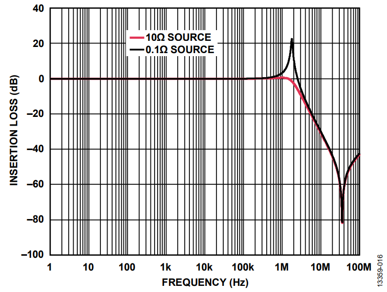
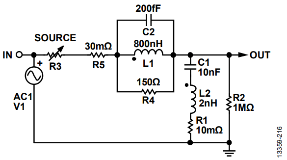
Other factors that have an effect on the resonant peaks are the series and load impedances of the ferrite bead filter. Figure 19 shows the circuit simulation result comparing a 10 Ω resistor and a 0.1 Ω series source resistor. Peaking significantly reduces and damps for higher source resistance. However, the load regulation degrades with this approach, making it unrealistic in practice. The dc voltage at the load droops with load current due to the drop from the series resistance.


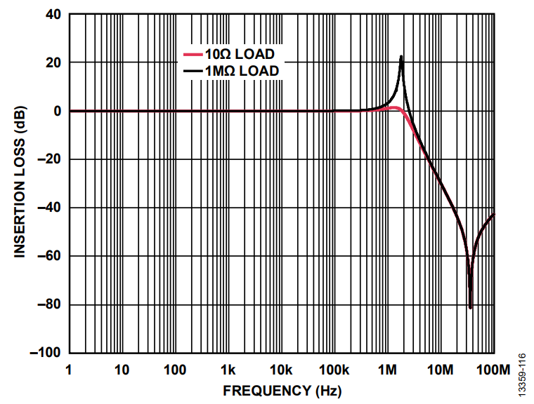
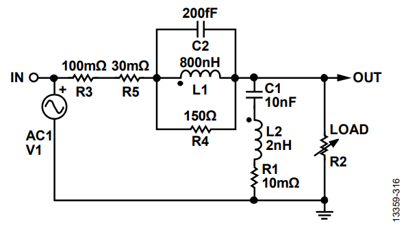
Load impedance also affects the peaking response. Peaking is worst for light load conditions.
Figure 21 shows a circuit simulation changing from a 1 MΩ load to a 10 Ω load using the same source resistance. Peaking is significantly reduced and damped for lower load resistance. Note that in actual applications (see Figure 13), higher dc load current significantly affects ferrite bead performance. The inductance of the bead drops as dc current increases and affects the resonant frequency cutoff.


Damping Methods
This section describes three damping methods that a system engineer can use to reduce the level of resonant peaking significantly (see Figure 23).

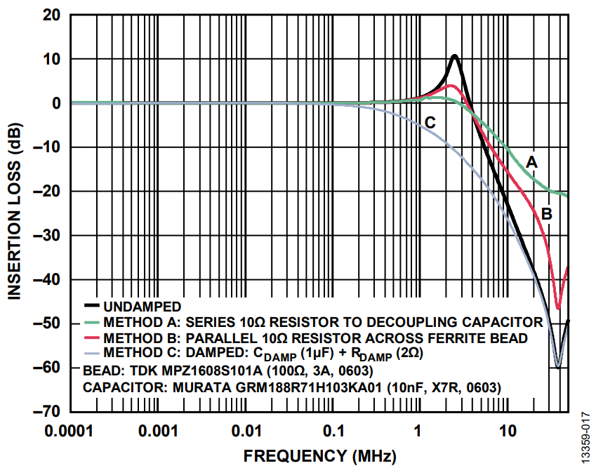
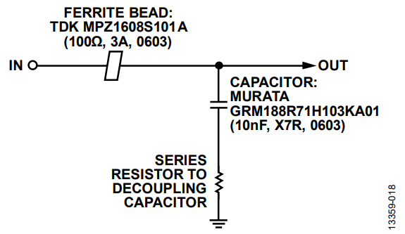
Method A consists of adding a series resistor to the decoupling capacitor path (see Figure 24), which dampens the resonance of the system but degrades the bypass effectiveness at high frequencies.

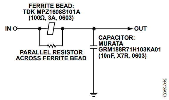
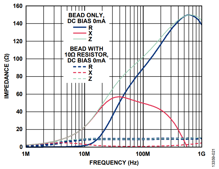
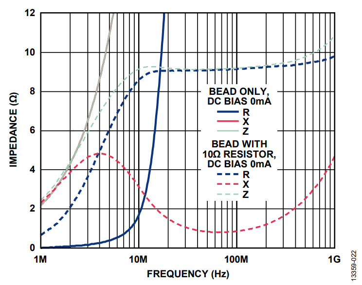
Method B consists of adding a small parallel resistor across the ferrite bead (see Figure 25), which also dampens the resonance of the system. However, the attenuation characteristic of the filter is reduced at high frequencies. Figure 26 and Figure 27 show the impedance vs. frequency curve of the MPZ1608S101A with and without a 10 Ω parallel resistor. The green dashed curve is the overall impedance of the bead with a 10 Ω resistor in parallel. The impedance of the bead and resistor combination is significantly reduced and is dominated by the 10 Ω resistor. However, the 3.8 MHz crossover frequency for the bead with the 10 Ω parallel resistor is much lower than the crossover frequency of the bead on its own at 40.3 MHz. The bead appears resistive at a much lower frequency range, lowering the Q for improved damped performance.


Method C consists of adding a large capacitor (CDAMP) with a series damping resistor (RDAMP), which is often optimum (see Figure 28).

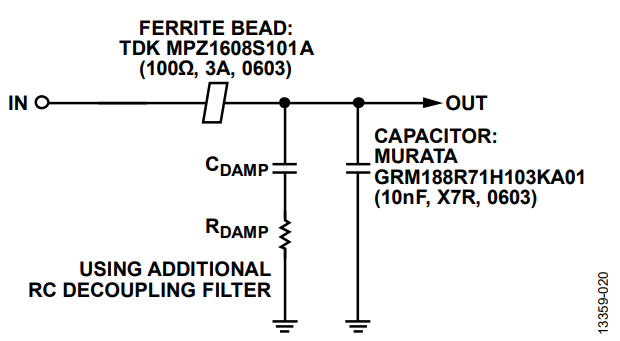
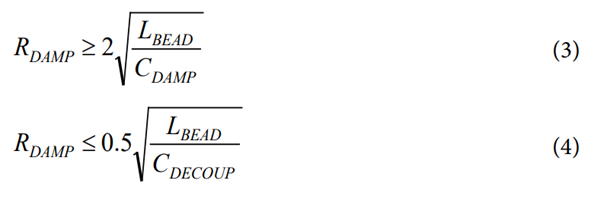
Adding the capacitor and resistor dampens the resonance of the system and does not degrade the bypass effectiveness at high frequencies, as shown in Figure 23. Implementing this method avoids excessive power dissipation on the resistor due to a large dc blocking capacitor. The capacitor must be much larger than the sum of all decoupling capacitors, which reduces the required damping resistor value. The capacitor impedance must be sufficiently smaller than the damping resistance at the resonant frequency to reduce the peaking. Determine the RDAMP range by using Equation 3 and Equation 4. Using a ratio of 16 or higher between damping capacitance (CDAMP) and decoupling capacitance (CDECOUP) provides a range of damping resistance that satisfies both equations.
where:
RDAMP is the damping resistance.
LBEAD is the bead inductance from Equation 1, including external inductance such as the parasitic trace inductance of the board.
CDAMP is the damping capacitance.
CDECOUP is the decoupling capacitance.
Figure 29 shows the ADP5071 positive output spectral plot with Method C damping implemented on the application circuit shown in Figure 17. The CDAMP and RDAMP used are a 1 μF ceramic capacitor and a 2 Ω SMD resistor, respectively. The fundamental ripple at 2.4 MHz is reduced by 5 dB as opposed to the 10 dB gain shown in Figure 18.

Generally, Method C is the most elegant and is implemented by adding a resistor in series with a ceramic capacitor rather than buying an expensive dedicated damping capacitor. The safest designs always include a resistor that can be tweaked during prototyping and that can be eliminated if not necessary. The only drawbacks are the additional component cost and greater required board space.
Conclusion
This application note shows key considerations that must be taken into account when using ferrite beads. The application note also details a simple circuit model representing the bead. The simulation results show good correlation with the actual measured impedance vs. the frequency response at zero dc bias current.
The application note also discusses the effect of the dc bias current on the ferrite bead characteristics. It shows that a dc bias current greater than 20% of the rated current can cause a significant drop in the bead inductance. Such a current can also reduce the effective impedance of the bead and degrade its EMI filtering capability. When using ferrite beads in supply rail with dc bias current, ensure that the current does not cause saturation of the ferrite material and produce significant change of inductance.
Because the ferrite bead is inductive, do not use it with high Q decoupling capacitors without careful attention. Doing so can do more harm than good by producing unwanted resonance in a circuit. However, the damping methods proposed in this application note offer an easy solution by using a large decoupling capacitor in series with a damping resistor across the load, thus avoiding unwanted resonance. Applying ferrite beads correctly can be an effective and inexpensive way to reduce high frequency noise and switching transients.
References
AN 583 Application Note. Designing Power Isolation Filters with Ferrite Beads for Altera FPGAs. Altera Corporation, 2009.
Applications Manual for Power Supply Noise Suppression and Decoupling for Digital ICs, Murata Manufacturing Co., Ltd., 2010.
Burket, Chris. All Ferrite Beads Are Not Created Equal – Understanding the Importance of Ferrite Bead Material Behavior. TDK Corporation, 2011.
Fancher, David B. ILB, ILBB Ferrite Beads: Electro-Magnetic Interference and Electro-Magnetic Compatibility (EMI/EMC). Vishay Dale, 1999.
Hill, Lee and Rick Meadors. Steward EMI Suppression Technical Presentation. Steward.
Kundert, Ken. Power Supply Noise Reduction. Designer’s Guide Consulting, Inc., 2004.
Solving Electromagnetic Interference (EMI) with Ferrites, Fair-Rite Products Corp.
Weir, Steve. PDN Application of Ferrite Beads. IPBLOX, LLC, 2011
Authors

