摘要
This application note explains how to use a microprocessor's UART to implement a 1-Wire® bus master. It includes an explanation of the required electrical interface, UART configuration, and timing relationship between the UART and 1-Wire signals. Additionally, it references the UART 1-Wire Master software utility, which generates both standard and overdrive speed timings to aide in development. The flexibility offered in setting up the UART byte timing allows the straightforward implementation of 1-Wire time slots as well as the Reset and Presence Detect pulses.
Introduction
Maxim’s innovative 1-Wire® protocol allows power delivery and digital communication across a single conductor plus a ground reference. 1-Wire devices provide economical solutions for identification, memory, time keeping, measurement, and control with an additional benefit of being able to operate at long distances (>100 meters). There are various methods to implement a 1-Wire host side driver such as using one of Maxim’s bridge devices, bit-banging a microcontroller’s GPIO, or using a peripheral such as a Universal Asynchronous Receiver Transmitter (UART) to generate the required timings. This application note discusses the UART implementation and describes how to use the UART 1-Wire Master software utility to aide in the development process. The application automatically configures the peripheral data for a wide range of baud rates needed to realize each timing parameter.
The typical data rate of 16kbps is more than sufficient for the intended tasks as most 1-Wire devices provide relatively small amounts of data. It is often convenient to use a general-purpose input/output (GPIO) pin of an 8-bit or 16-bit microcontroller in a ‘bit banging’ manner to act as the bus master.
However, processor clock frequencies in many 32-bit systems routinely exceed 100MHz. Using a GPIO pin as the 1-Wire bus master consumes a large number of clock cycles per 1-Wire bit. Its edges may not be precisely controlled to meet the necessary timing requirements. Precious battery power is consumed in 32-bit portable systems while generating the 1-Wire read and write time slots. The burden of bit timing and byte framing operations from the main processor can be offloaded if a UART peripheral is available.
This application note includes an explanation of the required electrical interface, UART configuration, and timing relationship between the UART and 1-Wire signals. A general understanding of 1-Wire communication is assumed. Typical timing and logic levels are used in the following discussion. Refer to the 1-Wire device data sheets for specific timing and voltage specifications and tolerances.
Conceptual Overview
A UART with various baud rates provides the output timing necessary to implement a 1-Wire master if it is properly configured with respect to baud rate, data bits per character, parity, and number of stop bits. Varying the UART transmit byte values produces the 1-Wire Reset pulse, as well as read and write slots to build the low-level commands. The microprocessor simply puts one-byte character codes into the UART transmit register to initiate a 1-Wire timing pattern. Conversely, the microprocessor reads single-byte character codes corresponding to a 1 or 0 bit read from a 1-Wire slave. All 1-Wire bit transfers require the bus master (i.e. UART peripheral) to initiate the timing cycle by driving the 1-Wire bus low. A byte must be simultaneously transmitted and received by the UART to generate 1-Wire timing. Therefore, the peripheral must support full-duplex operation. The received byte provides useful information, which can identify a successfully transmitted data byte, shorted connection, data corruption, or if a 1-Wire slave device is connected. Each transmitted byte corresponds to a single 1-Wire read bit, write bit, or Reset.
UART to 1-Wire Electrical Interface
1-Wire devices operate in an open-drain environment on bus voltages ranging from 1.8V to 5.5V. Exact logic levels and minimum pullup voltages are device dependent. So, refer to the device data sheet for compatible operating voltages. Figure 1 shows a possible configuration if the host’s output voltage on the TX pin is within the slave’s operating voltage. The pullup voltage (VPUP) from the TX pin provides the voltage to the top of the pullup resistor (RPUP) while the RX pin’s high impedance input maintains the open-drain configuration. This allows slave devices to pull the 1-Wire IO line low during a read bit or a Reset Presence Pulse while the TX signal is high. Selecting an RPUP value is important for proper operation as the configuration in Figure 1 does not have a provision for a strong pullup. The amount of current being delivered to a slave device for commands (i.e. copy scratchpad) requiring extra current must be considered. The resistor must be small enough to deliver the required current while preventing the voltage drop from violating the slave’s minimum operating voltage or VIL level for both the host and slave. A 480Ω resistor is typically a good starting point for the pullup on the 1-Wire data line for this configuration. Use an independent pullup voltage connection (Figure 2 and Figure 3) for systems where the voltage on the host’s TX pin is not directly compatible.
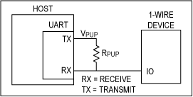
Figure 1. 1-Wire bus interface circuitry.
An external open-drain buffer circuit is usually needed as most UART transmit data pins are not open-drain. This circuit can be constructed out of discrete components (Figure 2) or integrated solutions such as the Fairchild NC7WZ07 (Figure 3). The 4.7kΩ pullup resistor is a good starting point for ROM level commands in both the circuits but must be resized to allow high current operations such as copying data to an EEPROM. It is important to verify that the logic levels do not violate EC table parameters for both the host and slave.

Figure 2. Discrete open-drain buffer.

Figure 3. Integrated open-drain buffer.
1-Wire/UART Bit Timing
The timing diagrams in Figures 5 to 9 describe the relationship between the 1-Wire time slots and corresponding UART byte frame. The UART serves as the bus master, and therefore begins all communication on a high-to-low transition of the TX output pin. The UART receives a byte for every byte transmitted as the electrical interface ties the buffered TX signal to the RX input pin.
Each diagram includes a UART configuration, transmit byte value, and expected receive byte value. The listed UART configurations produce waveforms compliant with regular mode 1-Wire timings. Note that the UART is configured with a different baud rate for the Reset and Presence Pulse detect than with the read- and write-time slots. It is possible to use other configurations as well, although the evaluation criteria can be different from those in the timing diagrams. The transmit byte value corresponds to the 1-Wire bus master role, and the receive byte value or range represents the expected activity on the bus. The receive value must be evaluated to determine the bit value returned by the 1-Wire slave device when performing a read. The read 0 and read 1 evaluation criteria are included in the diagrams.

Figure 4. Timing diagram legend.
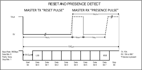
Figure 5. Reset pulse and presence detect.
Multiple baud rates can be used to generate a 1-Wire Reset and detect the Presence Pulse. Figure 5 shows the UART configuration with a baud rate of 9600 to create a stand speed 1-Wire Reset. Each UART bit’s time slot is calculated with the inverse of the baud rate (1/baud rate). The UART’s start bit, as it is always low, can be used in combination with the eight data bits to develop the appropriate timing. The UART data is transmitted as a least significant bit first. Transmitting a byte of F0h makes data bits 0 to 3 a logic 0 and data bits 4 to 7 a logic 1, which creates a Reset Low Time (TRSTL) of 520.83us. The receive value depends on the presence of one or more 1-Wire slave devices, the internal timing of each slave device’s Present Pulse, rise times, and the UART's sampling time within each bit window. The receive value equals the transmit value if no device is present. The receive value varies when a device is present. A single slave device running at a minimum internal timing may respond with E0h, while one with maximum internal timing may return a value of 90h. It is important to confirm timings with an oscilloscope or logic analyzer to ensure the desired timing was achieved. It is important to confirm all timings since UART peripherals have different error rates for each baud rate.
A delay may need to be added between the UART bytes being transmitted to allow for the required recovery time (TREC). Do not stack up commands to be transmitted consecutively in the host’s UART buffer if these delays are required. The UART 1-Wire Master utility simplifies the task by calculating the TX, RX, and delay values for each timing parameter for the selected baud rate. A link to this software utility is provided at the end of this document. This utility provides the UART configuration for both standard and overdrive timings for numerous baud rates. Use the help menu in the utility for a detailed description.
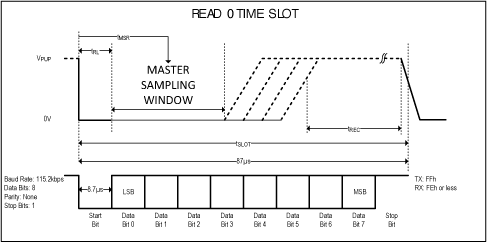
Figure 6. Read 0 time slot.
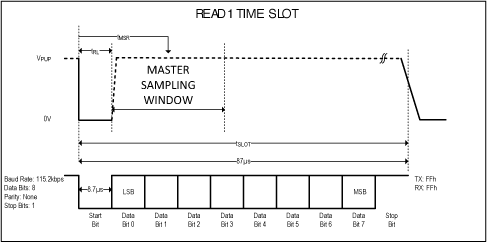
Figure 7. Read 1 time slot.
The host always initiates communication in a 1-Wire system as mentioned earlier. The host pulls the 1-Wire IO low for a duration of Read Low Time (TRL) to read a bit from the slave. The slave holds the IO low past the Master Read Sample Time (TMSR) if it is transmitting a 0-bit and does nothing when sending a 1-bit, allowing the IO to float after the host releases the line at the end of TRL. The read time slots generated in Figures 6 and 7 use a baud rate of 115,200. The RX byte received from a 1-Wire read 0 ranges from 0xFE to 0x00 depending on the internal time base of the slave device and IO rise time. The RX byte received from a 1-Wire read 1 is always 0xFF (for 115,200 baud) as the 1-Wire slave allows the data line to return to a 1 state as soon as the bus master releases it. The transmit and receive bytes can vary as the baud rate is increased. The UART 1-Wire Master utility calculates the appropriate TX, RX, and delay value for the selected baud rate.
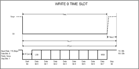
Figure 8. Write 0 time slot.
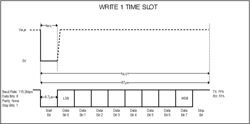
Figure 9. Write 1 time slot.
Figures 8 and 9 show how to transmit a 1 or 0 to the slave device at a baud rate of 115,200. However, there are numerous baud rates that can generate the appropriate timing. Again, the UART 1-Wire Master utility can calculate the appropriate values. It seems unnecessary to evaluate the RX byte for 1-Wire writes when reviewing the figures as the IO line is solely driven by the host and the slave device does not respond with any data. However, evaluating the RX value and ensuring it matches the TX value confirms there is no data corruption. Some 1-Wire systems have slave devices that can be added to the system during normal operation. An attached device would produce some unwanted transitions on the bus if added during a write. Checking the RX values catches this problem.
1-Wire Bit-to-Bit Timing
A key advantage of the 1-Wire bus is the flexibility in the bit-to-bit timing. The delay between bits can be as short as TREC minimum, or as long as the bus master deems necessary. There is no maximum delay period between the 1-Wire bits or bytes. Therefore, the processor can service the UART at its leisure in framing bit time slots into byte values. The communication with 1-Wire devices can be designated a low-priority task. The processor need not waste processing cycles or power, or neglect high-priority, time-critical tasks.
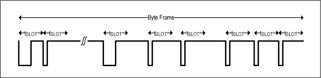
Figure 10. Bit-to-bit timing flexibility.
UART 1-Wire Master Utility
The UART 1-Wire Master utility quickly determines what TX, RX, and delays are needed to generate 1-Wire timings across various baud rates. The utility allows communication with USB to UART bridge devices manufactured by Prolific or FTDI, allowing real-time communication with 1-Wire slave devices. An emulation option can be selected if the hardware is not available. The configuration tab in Figure 11 provides fields to enter the EC table timing parameters. These values are used to calculate the UART data. The 1-Wire tab confirms proper operation with a real slave device or with a simulated output when the hardware is not connected. The data log displays pertinent information for each executed command. Select the User’s Guide from the help menu to use this tool.
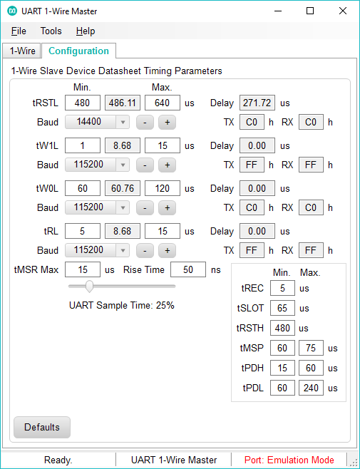
Figure 11. Configuration tab.

Figure 12. 1-Wire tab.
Conclusion
The UART remains a valuable peripheral in modern processors because of its programmability. The flexibility in setting up the UART byte timing allows the straightforward implementation of 1-Wire read/write time slots as well as the detection of Reset and Presence Pulse.
The UART 1-Wire Master software utility can generate timing for both regular and overdrive speeds for all timing parameters, allowing for rapid development. The tool supports a wide range of baud rates ensuring compatibility with most, if not all, UART peripherals. The software utility can be downloaded from DS1990R.
Trademarks
1-Wire is a registered trademark of Maxim Integrated Products, Inc.
FTDI is a registered trademark of Future Technology Devices International.
Prolific is a registered trademark of Prolific Technology, Inc.


