Understanding IP2 and IP3 Issues in Direct Conversion Receivers for WCDMA Wide Area Basestations
Understanding IP2 and IP3 Issues in Direct Conversion Receivers for WCDMA Wide Area Basestations
2024-12-19
Introduction
A direct conversion receiver architecture offers several advantages over the traditional superheterodyne. It eases the requirements for RF front end bandpass filtering, as it is not susceptible to signals at the image frequency. The RF bandpass filters need only attenuate strong out-of-band signals to prevent them from overloading the front end. Also, direct conversion eliminates the need for IF amplifiers and bandpass filters. Instead, the RF input signal is directly converted to baseband, where amplification and filtering are much less difficult. The overall complexity and parts count of the receiver are reduced as well.
Direct conversion does, however, come with its own set of implementation issues. Since the receive LO signal is at the same frequency as the RF signal, it can easily radiate from the receive antenna and violate regulatory standards. Also, a thorough understanding of the impact of the IP2 and IP3 issues is required. These parameters are critical to the overall performance of the receiver and the key component is the I/Q demodulator.
Unwanted baseband signals can be generated by 2nd order nonlinearity of the receiver. A tone at any frequency entering the receiver gives rise to a DC offset in the baseband circuits. Once generated, straightforward elimination of DC offset becomes very problematic. That is because the frequency response of the post-down conversion circuits must often extend to DC. The 2nd order nonlinearity of the receiver also allows a modulated signal—even the desired signal—to generate a pseudo-random block of energy centered about DC.
Unlike superheterodyne receivers, direct conversion receivers are susceptible to such 2nd order mechanisms regardless of the frequency of the incoming signal. So minimizing the effect of finite 2nd order linearity is critical.


Later in this article we consider the effect of 3rd order distortion on a direct conversion receiver. In this case, two signals separated by an appropriate frequency must enter the receiver in order for unwanted products to appear at the baseband frequencies.
Second Order Distortion (IP2)
The second order intercept point (IP2) of a direct conversion receiver system is a critical performance parameter. It is a measure of second order non-linearity and helps quantify the receiver’s susceptibility to single- and 2-tone interfering signals. Let’s examine how this nonlinearity affects sensitivity.


We can model the transfer function of any nonlinear element as a Taylor series:
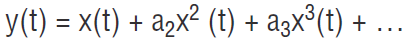
where x(t) is the input signal consisting of both desired and undesired signals. Consider only the second order distortion term for this analysis. The coefficient a2 is equal to
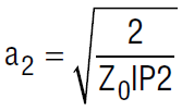
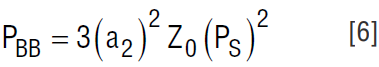
where IP2 is the single tone intercept point in watts. Note that the 2-tone IP2 is 6dB below the single-tone IP2. The more linear the element, the smaller a2 is.
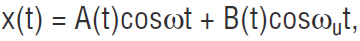
Every signal entering the nonlinear element generates a signal centered at zero frequency. Even the desired signal gives rise to distortion products at baseband. To illustrate this, let the input signal be represented by x(t) = A(t)cosωt, which may be a tone or a modulated signal. If it is a tone, then A(t) is simply a constant. If it is a modulated signal, then A(t) represents the signal envelope.
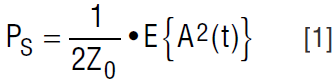
By definition, the power of the desired signal is
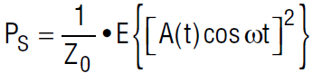
where E{β} is the expected value of β. Since A(t) and cosωt are statistically independent, we can expand E{(A(t)cosωt)2} as E{A2(t)} • E{cos2ωt}. By trigonometry
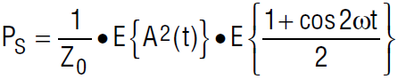
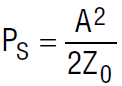
The expected value of the second term is simply ½, so the power of the desired signal simplifies to:
In the case of a tone, A(t) may be replaced by A. The signal power is, as expected, equal to
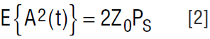
In the more general case, the desired signal is digitally modulated by a pseudo-random data source. We can represent it as bandlimited white noise with a Gaussian probability distribution. The signal envelope A(t) is now a Gaussian random variable. The expected value of the square of the envelope can be expressed in terms of the power of the desired signal as:
Now substitute x(t) into the Taylor series expansion to find y(t), which is the output of the nonlinear element:
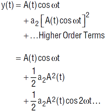
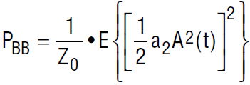
Consider the 2nd order distortion term ½a2[A(t)]2. This term appears centered about DC, whereas the other 2nd order term appears near the 2nd harmonic of the desired signal. Only the term near DC is important here, as the high frequency tone is rejected by the baseband circuitry.
In the case where the signal is a tone, the 2nd order result is a DC offset equal to:

If the desired signal is modulated, then the 2nd order result is a modulated baseband signal. The power of this term is
This can be expanded to:
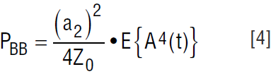
In order to express this result in terms of the desired signal power, we must relate E{A4(t)} to E{A2(t)}. For a Gaussian random variable, the following relation is true:
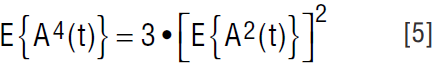
The distortion power can then be expressed as
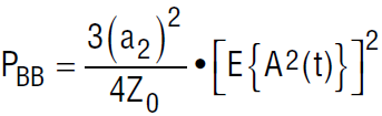
Now express the expected value in terms of the desired signal power:
It is the conversion of any given tone to DC, and any modulated signal into a baseband signal that makes 2nd order performance critical to direct conversion receiver performance. Unlike other nonlinear mechanisms, the signal frequency does not determine where the distortion product falls.
Any two signals entering the nonlinear element give rise to a beat note/term. Let
where the first term is the desired signal and the second term is an unwanted signal.
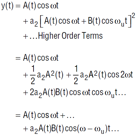
The second order distortion term of interest is a2A(t)B(t)cos(ω – ωu)t. This term describes the distortion product centered about the difference frequency between the two input signals. In the case of two unwanted tones entering the element, the result includes a tone at the difference frequency. If the two unwanted signals are modulated, then the resultant includes a modulated signal centered about their difference frequency.
We can apply these principles to a direct conversion receiver example. Figure 1 shows the block diagram of a typical WCDMA basestation receiver. Here are some key characteristics of this example:
- Basestation Type: FDD, Band I
- Basestation Class: Wide Area
- Number of carriers: 1
- Receive band: 1920MHz to 1980MHz
- Transmit band: 2110MHz to 2170MHz
The RF section of this receiver includes a diplexer, a bandpass filter, and at least one Low Noise Amplifier (LNA). The frequency selective elements are used to attenuate out-of-band signals and noise. The LNA(s) establishes the noise figure of the receiver. The I/Q demodulator converts the receive signal to baseband.
In the examples illustrated below, the characteristics of the LT5575 I/Q demodulator as representative of a basestation class device of this type. Lowpass filters and baseband amplifiers bandlimit and increase the signal level before it is passed to the A/D converters. The diplexer and RF bandpass filter serve as band filters only; they do not offer any carrier selectivity.
The second order linearity of the LNA is much less important than that of the demodulator. This is because any LNA distortion due to a single signal is be centered about DC and rejected by the demodulator. If there are two unwanted signals in the receive band (1960MHz, for example), then a second order product is generated by the LNA at the difference frequency. This signal is demodulated and appears as a baseband artifact at the A/D converter. We need not address this condition, however, because out of band signals emerging from the front end diplexer are not strong enough to create distortion products of any importance.
Consider first a single unmodulated tone entering the receiver (see Figure 2). As detailed above, this tone gives rise to a DC offset at the output of the demodulator. If the baseband cascade following the demodulator is DC-coupled, this offset is applied to the A/D converter, reducing its dynamic range. The WCDMA specification (3GPP TS 25104.740) calls out an out-of-band tone at –15dBm, located 20MHz or more from either receive band edge (section 7.5.1). Compute the DC offset generated in the I/Q demodulator:
- Tone entering receive antenna port: –15dBm
- Diplexer rejection at 20MHz offset: 0dB
- Bandpass rejection at 20MHz offset: 2dB
- RF gain preceding LT5575: 20dB
- Tone entering LT5575: 3dBm
- LT5575 IIP2, 2-tone: 60dBm
- LT5575 a2: 0.00317
- DC offset at LT5575 output: 0.32mV
- Baseband voltage gain: 31.6
- DC offset at A/D input: 10mV
Single WCDMA carriers can also serve as interferers, as detailed in section 7.5.1. In one case, this carrier is offset by at least 10MHz from the desired carrier, but is still in the receive band. The power level is –40dBm, and the receiver must meet a sensitivity of –115dBm for a 12.2kbps signal at a BER of 0.1%. Here are the details:
- Signal entering receive antenna port: –40dBm
- RF gain preceding LT5575: 20dB
- Signal entering LT5575: –20dBm
- LT5575 IIP2, 2-tone: 60dBm
- LT5575 a2: 0.00317
A MATLAB simulation performed using a pseudo-random channel predicts a distortion at the LT5575 output of –98.7dBm. This result agrees well with that given by equation 6, which predicts a distortion power of –98.2dBm.
The baseband product that appears at the LT5575 output is a noiselike signal, created from the interfering WCDMA carrier. If this signal is large enough, it can add to the thermal receiver and A/D converter noise to degrade sensitivity. Compute the equivalent thermal noise at the receiver input with no added distortion:
- Sensitivity: –121dBm
- Processing + coding gain: 25dB
- Signal to noise ratio at sensitivity: 5.2dB
- Thermal noise at receiver input: –101.2dBm
Now refer the distortion signal back to the receiver input:
- RF gain preceding LT5575: 20dB
- Equivalent interference level at Rx input: –118.7dBm
The baseband second order product in this case is 17.5dB below the thermal noise at the receiver input. The resulting degradation in sensitivity is <0.1dB, so the receiver easily meets the specification of –115dBm. This is illustrated in Figure 3. Single WCDMA carriers can also appear out of band, as specified in section 7.5.1. These can be directly adjacent to the receive band at levels as high as –40dBm. Here again, the second order effect of such carriers upon sensitivity is negligible, as the preceding analysis shows.


Another threat to sensitivity comes from transmitter leakage in FDD systems, as shown in Figure 4. In an FDD system, the transmitter and receiver are operating at the same time. For the WCDMA Band I case, the transmit band is 130MHz above the receive band. A single antenna is commonly used, with the transmitter and receiver joined by a diplexer. Here are some typical basestation coupled resonator-type diplexer specifications:
- Isolation, Tx to Rx 2110MHz: 55dB
- Diplexer insertion loss, Tx path: 1.2dB


In the case of a Wide Area basestation, the transmit power may be as high as 46dBm. At the transmit port of the diplexer the power is at least 47dBm. This high level modulated signal leaks to the receiver input, and some portion of it drives the I/Q demodulator:
- Receiver input power: –8dBm
- Rx BPF rejection at 2110MHz: 40dB
- RF gain preceding LT5575: 20dB
- Signal entering LT5575: –28dBm
- LT5575 IIP2, 2-tone: 60dBm
- LT5575 a2: 0.00317
A MATLAB simulation performed using a pseudo-random channel predicts the following:
- Distortion at LT5575 output: –114.7dBm
Refer this signal back to the receiver input:
- RF gain preceding LT5575: 20dB
- Equivalent interference level at Rx input: –134.7dBm
- Thermal noise at receiver input: –101.2dBm
This equivalent interference is 33.5dB below the thermal noise at the receiver input. The resulting degradation in sensitivity is <0.1dB, so the receiver easily meets the specification of –121dBm.
Third Order Distortion (IP3)
The third order intercept point (IP3) has an effect upon the baseband signal when two properly spaced channels or signals enter the nonlinear element.
Refer back to the transfer function: y(t) = x(t) + a2x2(t) + a3x3(t) + …, where x(t) is the input signal consisting of both desired and undesired signals. Consider now the third order distortion term. The coefficient a3 is equal to 2/(3Z0IP3) where IP3 is the single tone intercept point in Watts. Note that the 2-tone IP3 is 4.78dB below the single-tone IP3.
Two signals entering the nonlinear element generate a signal centered at zero frequency if the spacing between the two signals is equal to the distance to zero frequency. Let x(t) = A(t)cosωt + B(t)cosωut, where the first term is the desired signal and the second term is an unwanted signal. The unwanted signal may be a tone or a modulated signal. If it is a tone, then B(t) is simply a constant. If it is a modulated signal, then B(t) represents the signal envelope.
The output signal is then equal to y(t):
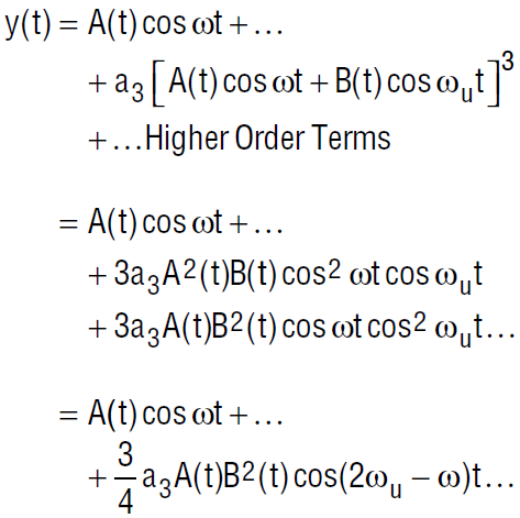
The third order distortion term of interest here is ¾a3A(t)B2(t)cos(2ωu – ω)t. In order for this distortion to appear at baseband, set ω = 2ωu. The power of the distortion is
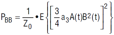
which can be expanded to
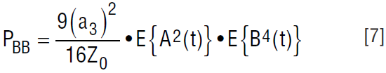
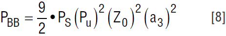
Consider the case of a modulated desired signal and a tone interferer; B(t) may be replaced by B. See Figure 5. The value of E{B4} can be expressed as (2Z0Pu) 2, where Pu is the power of the tone interferer. We can use Equation 2 to express E{A2(t)} in terms of the desired signal power as 2ZoPs, where Ps is the power of the desired signal. The power level of the distortion at baseband is then:


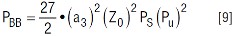
If the undesired signal is modulated, use Equations 2 and 5 to express E{B4(t)} as 3(2Z0Pu) 2, where Pu is the power of the tone interferer:
In the direct conversion receiver example, Section 7.6.1 of the WCDMA specification calls for two interfering signals as shown in Figure 6. One of these is a –48dBm CW tone, and the other is a –48dBm WCDMA carrier. These are offset in frequency so that the resulting 3rd order product appears centered about DC. Compute the intermodulation product generated in the I/Q demodulator:
- RF gain preceding LT5575: 20dB
- Signals entering LT5575: –28dBm
- LT5575 IIP3, 2-tone: 22.6dBm
- LT5575 a3: 0.0244


A MATLAB simulation performed using a pseudo-random channel predicts distortion at LT5575 output of –135.8dBm. This result agrees well with the equation 8, which predicts a distortion power of –135.7dBm.
Refer this signal back to the receiver input:
- RF gain preceding LT5575: 20dB
- Equivalent interference level at Rx input: –155.8dBm
- Thermal noise at receiver input: –101.2dBm
The equivalent interference in this case is 54.6dB below the thermal noise at the receiver input. The resulting degradation in sensitivity is <0.1dB, so the receiver easily meets the specification of –121dBm.
Conclusion
The calculations given here using the LT5575 I/Q demodulator show that a WCDMA wide area basestation receiver can be successfully implemented using a direct conversion architecture. The high 2nd order linearity and input 1dB compression point of the LT5575 are critical to meeting the performance requirements of such a design.
关于作者
Doug Stuetzle是凌力尔特公司高级模拟应用工程师。他于2003年加入该公司,为RF产品线中的有源混频器、解调器和检波器提供应用支持。他还设计并支持LTM9003、LTM9004、LTM9005和LTM9013 RF至数字接收器模块。这些模块设计用于满足各种数字通信标准的复杂要求,包括电路设计的各个方面,从GHz范围RF到中频,低至数字化输出位流。
现在他为各种
现在他为各种
关联至此文章


