Ultralow Power 14-Bit ADC Samples at 200ksps
Introduction
A new, versatile 14-bit ADC, the LTC1418, can digitize at 200ksps while consuming only 15mW from a single 5V supply. The LTC1418 is designed to be easy to use and adaptable, requiring little or no support circuitry in a wide variety of applications. Some of the key features of this new device include:
- 200ksps throughput
- Low power—15mW
- Single 5V or ±5V supplies
- 1.25LSB INL max and 1LSB DNL max
- Parallel and serial data output modes
- NAP and SLEEP power shutdown modes
- Small package—28-pin SSOP
High Performance without High Power
Figure 1 shows a block diagram of the LTC1418. This device includes a high performance differential sample-and-hold circuit, an ultra-efficient successive approximation ADC, an on-chip reference and a digital interface that allows easy serial or parallel interface to a microprocessor, FIFO or DSP. The LTC1418 is factory calibrated, so a lengthy calibration cycle is not required to achieve 14-bit performance. DC specifications include a 1LSB max differential linearity error (no missing codes) and 1.25LSB max integral linearity error guaranteed over temperature. The gain of the ADC is controlled by an on-chip 10ppm/°C reference that can be easily overdriven with an external reference if required.
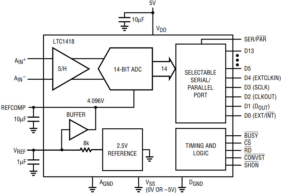
Figure 1. LTC1418 block diagram.
For AC applications, the dynamic performance of the LTC1418 is exceptional. The extremely low distortion differential sample-and-hold acquires input signals at frequencies up to 10MHz. At the Nyquist frequency, 100kHz, the spurious free dynamic range is typically 95dB. The noise is also low with a signal-to-noise ratio (SNR) of 82dB from DC to well beyond Nyquist.
The superior AC and DC performance of the LTC1418 doesn’t require a lot of power. In fact, the LTC1418 has the lowest power of any 14-bit ADC available, just 15mW at 200kHz (10mW at sample rates below 50kHz). Two shutdown modes make it possible to cut power further at lower sample rates.
High Impedance Inputs
The LTC1418’s high impedance inputs allow direct connection of high impedance sources without introducing errors. Many ADCs have a resistive input or input bias current that requires low source impedance to achieve low errors. Other ADCs with switched capacitor inputs exhibit large offset shifts when driven with high source impedance or a large source-impedance imbalance between their differential inputs. The unique sample-and-hold circuit of the LTC1418 has a low capacitance, high resistance (10MΩ||25pF) switched-capacitor input that has only 2LSB of offset shift with a source-impedance imbalance between 0Ω and 1M (see Figure 2a). (There is no shift if the input impedance is equal for +AIN and –AIN.) Connecting the ADC directly to a high impedance source avoids additional noise and offset errors that may be introduced by buffering circuitry. The only downside to directly connecting the ADC to a high source impedance is that the acquisition time will increase. The low input capacitance (20pF) of the LTC1418 allows full-speed operation with resistances up to 2k. Above 2k the sample rate must be lowered (see Figure 2b).
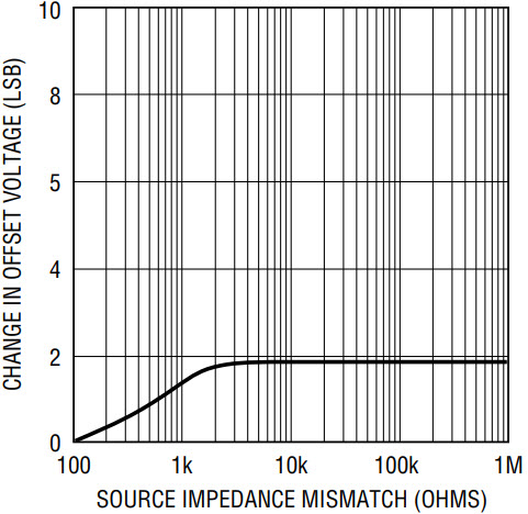
Figure 2a. Change in offset voltage with source impedance mismatch.
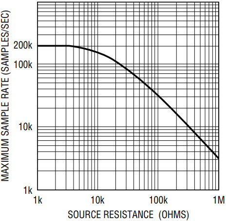
Figure 2b. Maximum sample rate vs unbuffered source resistance.
Differential Inputs with Wideband CMRR
The differential input of the LTC1418 has excellent common mode rejection, eliminating the need for some input-conditioning circuitry. Op amps and instrumentation amplifiers are often used to reject common mode noise from EMI, AC power and switching noise. Although these circuits perform well at low frequencies, their rejection at high frequencies deteriorates substantially. Figure 3 shows the CMRR of the LTC1418 vs frequency.
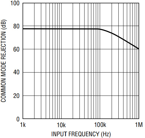
Figure 3. Input common mode rejection vs input frequency.
Single-Supply or Dual-Supply Operation
Single-supply ADCs can be cumbersome to work with in a dual-supply system. A signal with a common mode of zero volts has to be shifted up to the common mode of the ADC. Shifting the common mode can be accomplished with AC coupling, but DC information is lost. Alternatively, an op amp level shifter can be used, but this adds circuit complexity and additional errors. The LTC1418 can operate with single or dual supplies and allows direct coupling to the inputs in both cases. The ADC is equipped with circuitry that automatically detects when –5V is present at the VSS pin. With a –5V supply, the ADC operates in bipolar mode and the full-scale range becomes ±2.048V for +AIN with respect to –AIN. With a single supply, VSS = 0V and the ADC operates in unipolar mode with an input range of 0V to 4.096V.
On-Chip Reference
The on-chip reference of the LTC1418 is a standard 2.5V and is compatible with many system references; it is available on the REF output (pin 3). An internal amplifier boosts the 2.5V reference up to 4.096V; this sets the span for the ADC. The 4.096V output is available on the REFCOMP output (pin4) and may be used as a reference for other external circuitry. With a temperature coefficient of 10ppm/°C, both REF and REFCOMP are suited to serve as the master reference for the system. However, if an external reference circuit is required, its easy to overdrive either reference output. The 2.5V reference output is resistive (4k) and can be easily overdriven by any reference with low output impedance by directly connecting the external reference to the REF pin. If REFCOMP (the 4.096V reference) is to be overdriven, tie the REF pin to ground. This disables the output drive of the REFCOMP amplifier, allowing it to be easily overdriven.
Parallel Data Output for High Speed
The parallel output mode of the LTC1418 allows the lowest digital overhead. A microcontroller can strobe the ADC to start the conversion and perform other tasks while the conversion is running. The ADC will then signal the microcontroller after the conversion is complete with the BUSY signal, at which time valid data is available on the parallel output bus. BUSY may also be used to clock latches or a FIFO directly, since data is guaranteed to be valid with the rising edge of BUSY.
Serial Data Output for Minimal Wiring
The serial output mode of the LTC1418 is simple, requiring just three pins for data transfer: a data-out pin, a serial clock pin and a control pin. However, its simplicity doesn’t sacrifice flexibility. Serial data can be clocked with the internal shift clock for minimal hardware or an external shift clock for synchronization. Additionally, data can be clocked out during the conversion for the highest throughput rate or after the conversion for maximum noise immunity.
Perfect for Telecom: Wide Dynamic Range
Telecommunications systems require wide dynamic range. With its low noise and low distortion, the LTC1418 offers extremely wide dynamic range over its entire Nyquist bandwidth. Spurious free dynamic range is typically 95dB and only starts to drop off at input frequencies above Nyquist. The ultralow jitter of the sample-and-hold circuit, 5psRMS, keeps the SNR flat from DC to 1MHz, making this device useful for undersampling applications.
Another important requirement for telecom systems is a low error rate. In any ADC, there is a finite probability that a large conversion error (greater than 1% of full scale) will occur. In video or flash converters, these large errors are called “sparkle codes.” Large errors are a problem in telecom systems such as ISDN, because they result in errors in data transmission. All ADCs have a rate at which errors occur, referred to as the error rate. The error rate is dependent on the ADC architecture, design and process. Error rates vary greatly and can be as low as 1 in 10 billion to as high as 1 is 1 million. Telecom systems typically require error rates to be 1 in 1 billion or better.
The LTC1418 is designed to have ultralow error rates. The error rate is so low that it is difficult to measure because of the time in between errors. To make measurement more practical, the error rate was measured at an elevated temperature of 150°C, because error rate increases with temperature. Even at this high temperature, the error rate was 1 in 100 billion. The projected error rate at room temperature is 1 in 2,000,000 billion or about 1 error every 320 years if running at full conversion rate.
Ideal for Low Power Applications
LTC1418 is especially well suited for applications that require low power and high speed. The normal operating power is low—only 15mW. Power may be further reduced if there are extended periods of time between conversions. During these inactive periods when the ADC is not converting, the LTC1418 may be shut down. There are two power shutdown modes: NAP and SLEEP.
NAP mode shuts down 85% of the power and leaves only the reference and logic powered up. The LTC1418 can wake up from NAP mode very quickly; in just 500ns it can be ready to start converting. In NAP mode, all data-output control is functional; data from the last conversion prior to starting NAP mode can be read during NAP mode. RD also controls the state of the output buffers. NAP mode is useful for applications that must be ready to immediately take data after long inactive periods.
With slow sample rates, power can be saved by automatically invoking NAP mode between conversions. Referring to Figure 4, the SHDN pin and CONVST pin are driven together. A conversion will be started with the falling edge of this signal; once the conversion is completed, the ADC will automatically shut down. Before the next conversion can start, the CONVST and SHDN pins must be brought high early enough to allow for the 500ns wake-up time. Power drops with the sample frequency until it approaches the power of the reference circuit, about 2mW at frequencies less than 10kHz.
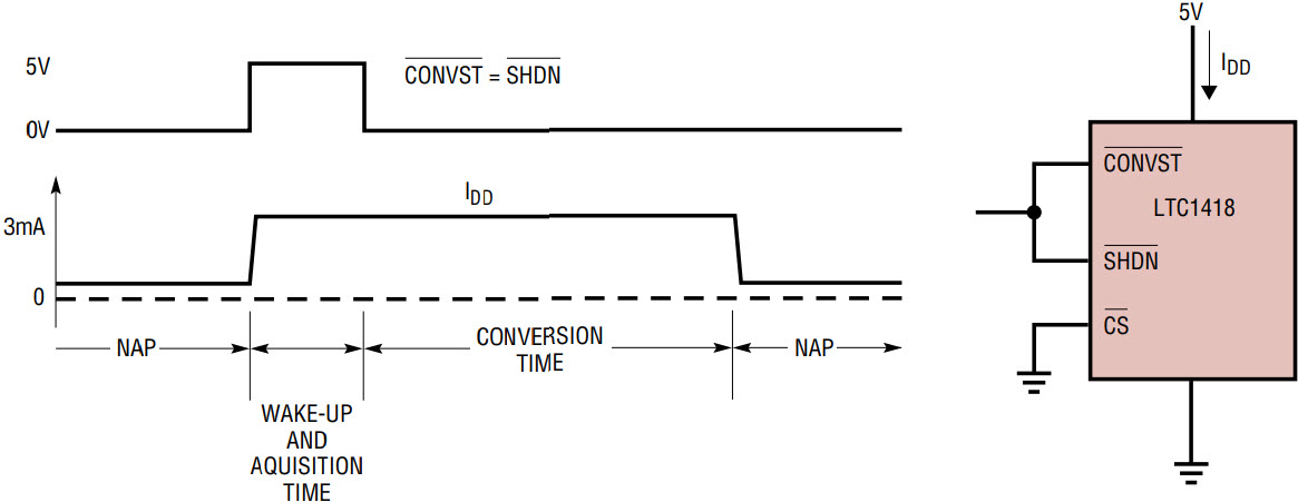
Figure 4a. NAP mode between conversions.
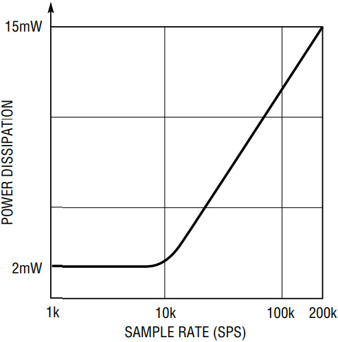
Figure 4b. Power dissipation vs sample rate with NAP mode between conversions.
The SLEEP mode is used when the NAP-mode current drain is too high or if wake-up time is not critical. In SLEEP mode, all bias currents are shut down, the reference is shut down and the logic outputs are put in a high impedance state. The only current that remains is junction leakage current, less than 1µA. Wake-up from the SLEEP mode is much slower, since the reference circuit must power up and settle to 0.01% for full accuracy. The wake-up time is also dependent on the value of the compensation capacitor used on the REFCOMP pin; with the recommended 10µF capacitor the wake up time is 10ms. SLEEP mode is useful for long inactive periods, that is, times greater than 10ms.
Conclusion
The new LTC1418 low power, 14-bit ADC will find uses in many types of applications, from industrial instrumentation to telephony. The LTC1418’s adaptable design reduces the need for expensive support circuitry. This can result in a smaller, lower cost system.


