ThinSOT RF Power Controllers Save Critical Board Space and Power in Portable RF Products
ThinSOT RF Power Controllers Save Critical Board Space and Power in Portable RF Products
2002-05-01
Introduction
The LTC4400-1 and LTC4401-1 provide RF power controller solutions for the latest cellular telephones. They feature very small footprints, low power consumption and wide frequency ranges while minimizing adjacent channel interference by carefully controlling RF power profiles. The LTC4400-1 and LTC4401-1 are both available in a low profile 6-pin ThinSOT package, and require few external parts. For example, when used with a directional coupler, only two resistors and two capacitors are required (Figure 1a, Figure 1b). Both devices require minimal power to operate, typically 1mA when enabled and 10μA when in shutdown.
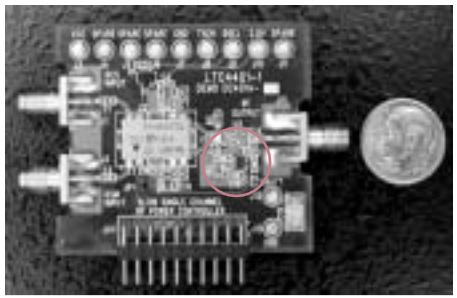
Figure 1a. The DC401A RF demo board. The circled area encloses the LTC4401 power controller (U4) and its required external components (C11, C12, C13 and R2).
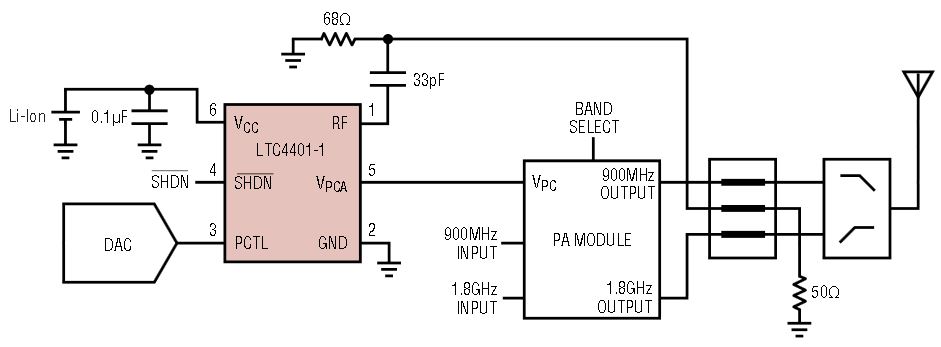
Figure 1b. Typical power control block diagram.
The LTC4400-1’s 450kHz loop bandwidth is optimized for applications involving fast turn-on (<2μs) and medium gain (200-300dB/V) RF power amplifiers. The LTC4401-1’s 250kHz loop bandwidth is optimized for slow turn-on (>2μs) and/or high gain (300-400dB/V) RF power amplifiers. The RF frequency range for both parts is 800MHz to 2.7GHz and the supply voltage range is 2.7V to 6.0V. This wide frequency and voltage range allow these products to be used in a variety of RF power control applications including GSM/GPRS, PCS and TDMA. The LTC4400-1 and LTC4401-1 include an auto zero system that requires periodic updates between single or multiple consecutive bursts. Therefore these power controllers are not suitable for continuous time applications.
Figure 2 shows the block diagram of the LTC4400/4401. When the part is in shutdown all circuitry except the reference is turned off and VPCA is held at ground. When the part is enabled, the auto zero system samples both internal and external offsets. After 10μs the auto zero system is disabled; the sampled offset voltage correction factor is held on two internal capacitors. A differential hold scheme is used to convert hold capacitor voltage droop (due to leakage currents) to a common mode voltage droop. This common mode voltage droop is rejected by the auto zero amplifier, resulting in greatly increased auto zero hold time. The auto zero system improves temperature dependent characteristics by removing temperature offset voltage drifts from internal and external sources.
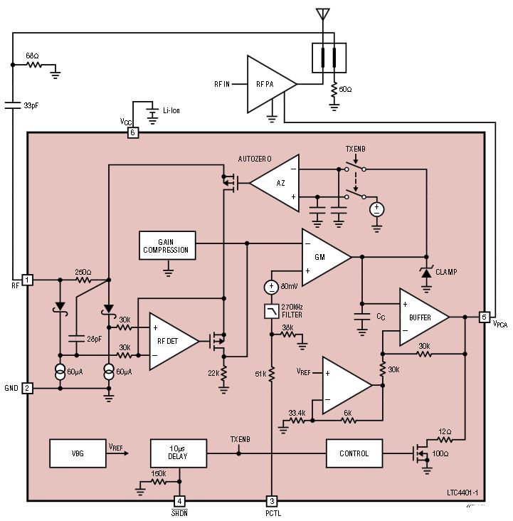
Figure 2. LTC4400/4401 block diagram.
The external power control ramp is applied 12μs after SHDNB is asserted high by the baseband microprocessor. When the ramp is applied, the VPCA voltage begins to rise. The RF power amplifier turns on when VPCA reaches the RF power amplifier’s threshold voltage. VPCA actually starts from 450mV. This start voltage reduces the time required to turn on the RF power amplifier and is lower than power amplifier threshold voltages used in mobile radio applications. The power control loop is open until the RF power amplifier turns on and starts supplying an RF output signal. While the loop is open, the VPCA rise time is limited by the LTC4400/4401 bandwidth and the magnitude of the PCTL signal. A portion of the RF output voltage is fed back to the LTC4400/4401 RF pin. This signal is then peak detected by an internal Schottky diode and capacitor. The detected voltage is applied to the negative input of the loop amplifier thereby closing the power control loop. Once the loop has closed, the RF output signal follows the power ramp signal at PCTL.
RF Detector Performance
The LTC4400 and LTC4401 incorporate two features to improve detector dynamic range. An auto zero system eliminates both internal offsets and external power control DAC offsets. Secondly, a compression circuit allows for higher feedback signals at lower RF power levels to extend the power detector range. The fully integrated detector has a small temperature coefficient as shown in Figure 3.
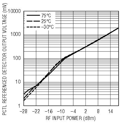
Figure 3a. Detector characteristics at 900MHz.
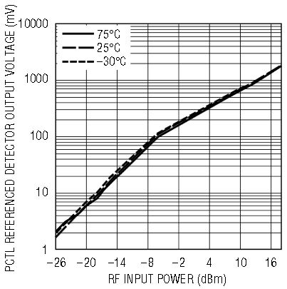
Figure 3b. Detector characteristics at 1800MHz.
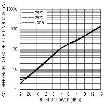
Figure 3c. Detector characteristics at 2400MHz.
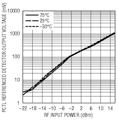
Figure 3d. Detector characteristics at 2700MHz.
Measuring RF Power Amplifier Rise Times
To determine which LTC RF power controller fits a particular application, the designer must first understand the RF power amplifier turn-on characteristics. Figure 4 shows a recommended test setup.
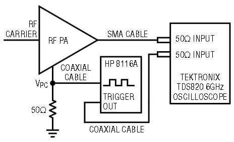
Figure 4. RF power amplifier rise time test setup.
A pulse generator is used to drive the RF amplifier power control pin, with its duty cycle set to minimize power dissipation (i.e. 1/8 duty cycle). Terminate the RF power control pin with a 50Ω resistor to match the pulse generator and avoid ringing. With a square wave pulse at various amplitudes, determine the RF output power response. Measure at several output power levels since the rise time may be power level dependent.
Use a high frequency digital scope to measure the RF output voltage shape. Figure 5 shows a typical RF output voltage response. This waveform consists of two regions, delay and ramp. The ramp time is measured from the start of the RF output to 90% of the final amplitude. Generally the LTC4400 is used for amplifiers with total delay and ramp times <2μs; the LTC4401 is used for amplifiers with total times >2μs. Other factors such as power amplifier gains, coupler and antenna switch losses, may also impact this selection. Very high gain power amplifiers may require the LTC4401 independent of the response times.
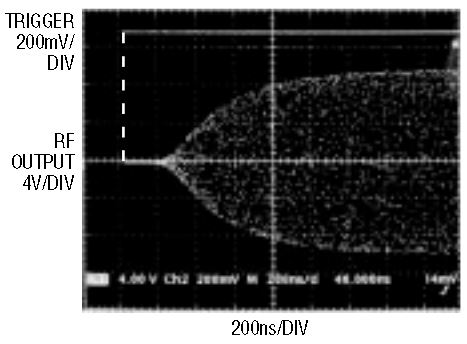
Figure 5. RF output voltage.
Powerful and Easy to Use Development Tools Optimize PA Control
Version 2 of the LT ramp-shaping program (LTRSv2.VXE) is available from Linear Technology. Figure 6 shows the program window of LTRSv2.VXE in ramp-shaping mode. This program lets users generate, reshape, and load ramp profile waveforms onto the DC314A digital demo board. The DC314A digital demo board provides regulated power supplies, control logic and a 10-bit DAC to generate the SHDNB signal and the power control PCTL signal. Flash memory and a serial port interface are also included for updating DAC profiles stored on the DC314A. Eight power control profiles can be stored in the flash memory. A rotary switch (SW1) can be used to select the desired power profile. The DC314A provides signals to the DC401A RF demo board, which contains a GSM/DCS RF channel, LTC4401-1 Thin-SOT power controller, and Hitachi PF08107B power amplifier (Figure 1B). The RF test measurement setup is shown in Figure 7.
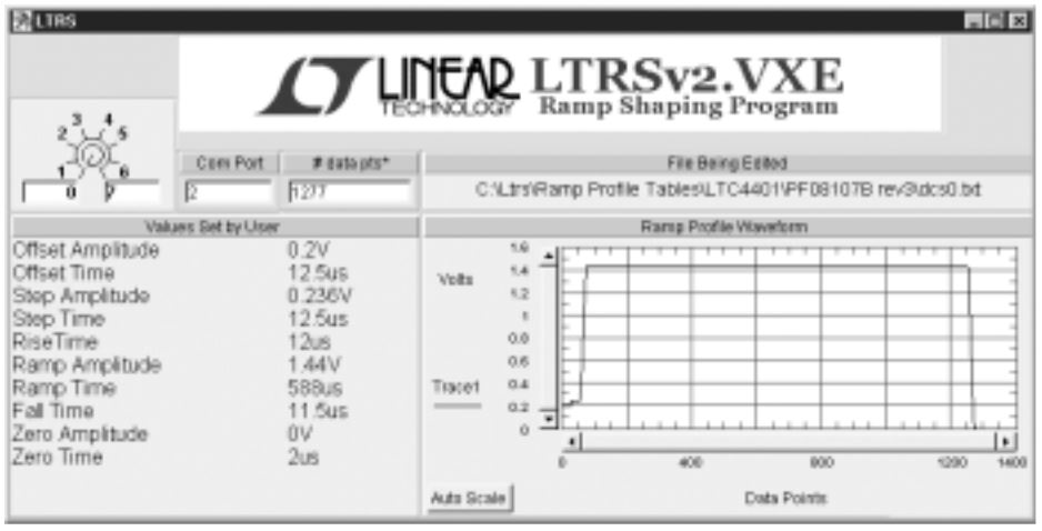
Figure 6. LTRSv2.vxe program window.
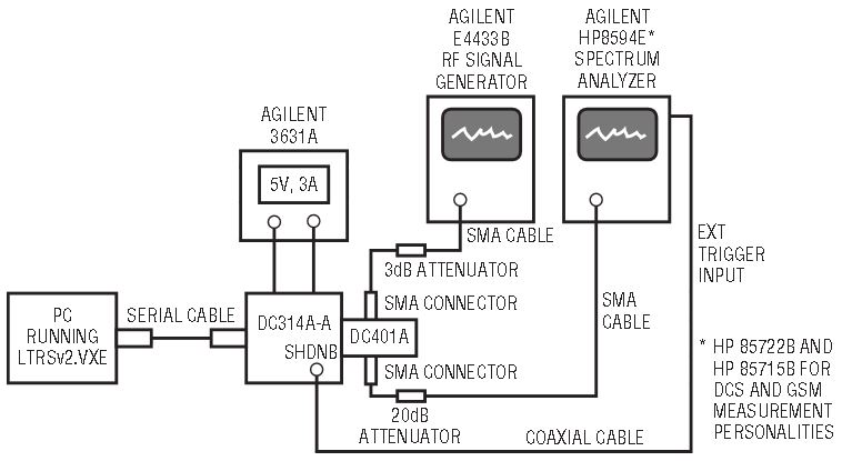
Figure 7. Demo board evaluation setup for GSM/DCS measurements.
LTRSv2.VXE creates smooth ramp waveforms based on user inputs. The user controls all aspects of the ramp parameters such as initial DAC offset, step voltage and time, rise and fall times, and maximum voltage amplitude and time. LTRSv2.VXE uses a raised-cosine function to create smooth transitions between areas of varying amplitudes, such as between the step and the maximum amplitude (Figure 8).

Figure 8. Rise and fall ramp shapes with raised-cosine function.
LTRSv2.VXE ramp profile parameters are saved in tables as text files. Linear Technology distributes LTRSv2.VXE with HP VEE Runtime, HP I/O Libraries, and ramp profile table templates for various power amplifiers. Each ramp profile waveform table can be edited or overwritten using LTRSv2.VXE. These ramp profile table templates serve as an excellent starting place for ramp-shaping. Figure 9 is an illustration of a typical ramp profile waveform with the ramp parameters labeled. Figure 10 shows the program window where the user changes ramp profile waveform parameters.
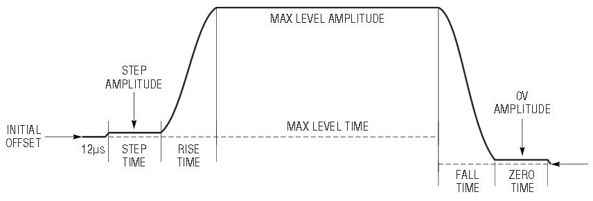
Figure 9. Typical ramp profile waveform.
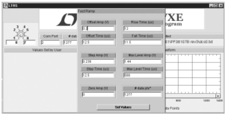
Figure 10. Ramp profile waveform parameter editing window.
Ramp shapes vary depending on which power controller and power amplifier are being used. For example, power amplifiers that exhibit “slow” turn-on/off times (2μs and greater) require larger step amplitude and time values and a higher DAC offset voltage. Similarly, rise and fall times for slow power amplifiers are longer.
Ramp-shaping is an iterative process. Changes should be made one parameter at a time since each affects different aspects of the output. Placing oscilloscope probes on PCTL and VPCA greatly facilitates the ramp-shaping process.
The ramp waveform begins with the DAC offset voltage. The offset improves ramp down characteristics of the power amplifier. A 100mV offset voltage is sufficient for the LTC4400-1 and fast power amplifiers, while a 200mV offset voltage is sufficient for the LTC4401-1 and slow power amplifiers. The offset time for the ramp is typically 12μs during which auto zeroing occurs. Figure 11 shows the timing relationship between SHDNB, VPCA and PCTL.
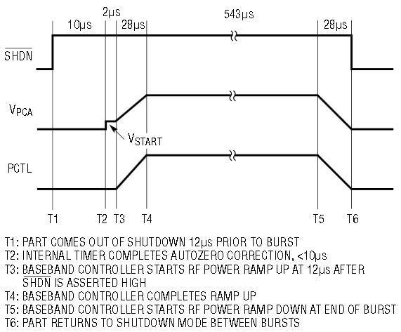
Figure 11. LTC4400/4401 timing diagram.
The first step in ramp-shaping is determining the correct output power. Increase or decrease the maximum amplitude to effect a corresponding change in the RF output power. Once the output power is set, adjust the initial step amplitude and time.
The initial step values are responsible for closing the voltage loop. VPCA must quickly rise to the RF power amplifier threshold voltage in order to meet power versus time specifications. If the initial step time or amplitude values are too low, the control voltage waveform will resemble VPCA in Figure 12. The resolution of the DAC allows for amplitude changes as small as 2mV. The step voltage can be changed in 1/2 microsecond multiples. There are some tradeoffs to take into consideration when choosing which parameters to change. For instance, if the step amplitude is too high, the RF output spectrum may exhibit spurs. However, if the step time is too long, as shown in Figure 13, meeting required power versus time is compromised because the time allotted for the burst portion is insufficient. Figure 14 shows the ideal shape for the control voltage. The rise portion of VPCA is smooth and has a constant slope until the maximum amplitude is reached.
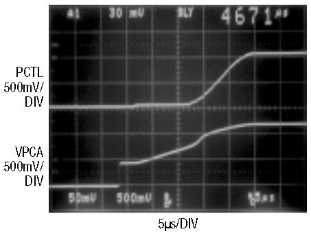
Figure 12. PCTL and VPCA waveforms with low ramp step amplitude and step time.
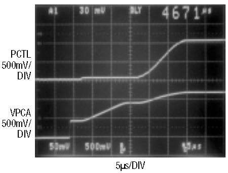
Figure 13. PCTL and VPCA waveforms with high ramp step amplitude and step time.
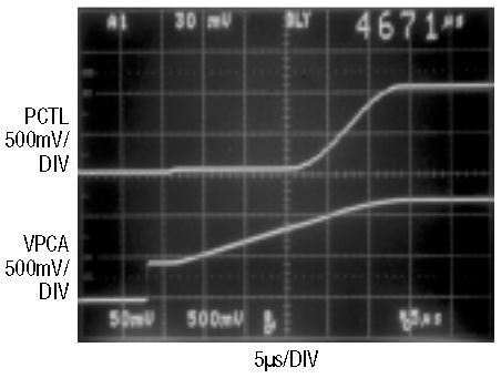
Figure 14. Optimized PCTL input and VPCA output.
Once the step values are set, the rise and fall times should be adjusted. If the rise time is too short for slow amplifiers, an overshoot will occur and will be visible in the power versus time measurement. Lengthening the fall time generally lowers the spurs ±400 kHz from the center frequency. Rise and fall times vary from 8μs–14μs.
The last step is adjusting the width of the maximum amplitude. This is necessary to meet power versus time specifications. Typically, the burst portion of the width is 588μs. The total time of the maximum ramp amplitude must be enough to pass the power versus time measurement and leave suitable time at 0 volts to turn the power amplifier off. Usually, 1μs is required to turn off a power amplifier.
After each parameter is changed, a graph of the waveform created appears in the program window along with the option to load the ramp onto the DC314A demo board.
Ramp-shaping is more challenging with slower power amplifiers because more time is required on the step, rise and fall. If there is not enough time to meet the power versus time mask and turn off the PA, then it is necessary to change the step amplitude and time. A change of 4mV to 6mV accounts for 1μs. Be careful to not let the step amplitude become too high to avoid spurs in the RF output.
Figure 15 shows the control voltage waveform for maximum output power at 1800MHz (DCS0). The waveform has an initial start voltage of 450mV. By starting the output control voltage at 450mV, the time required to reach the power amplifier threshold voltage is reduced. The start voltage is generated by the LTC4400/4401 and not by the program.
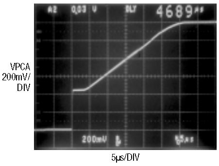
Figure 15. Correct VPCA response and 450mV start voltage.
Figure 16 is the corresponding output RF spectrum for the control voltage shown in Figure 15. The center frequency is 1710.2MHz and the input power to the power amplifier is 0dBm. Figure 17 shows the power versus time measurement. The onscreen table, shown in Figure 6, represents the values entered to create the ramp waveform. The input step and ramp amplitudes include a 200mV offset amplitude. Therefore, the actual step voltage is 36mV and the ramp amplitude voltage is 1.24V.
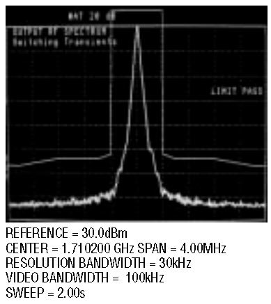
Figure 16. Output RF spectrum switching transients for DCS0.
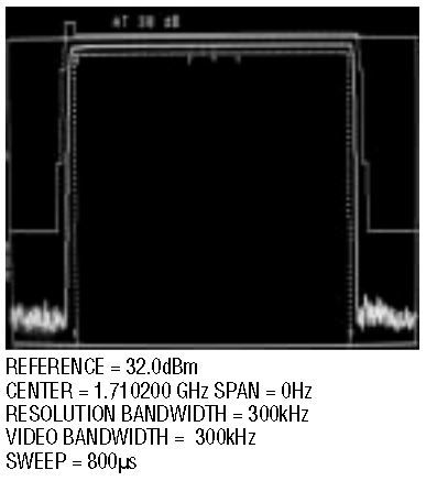
Figure 17. Power versus time measurement for DCS0.
Directional Coupler Alternatives
The DC401A board contains the LTC4401-1 power controller and Hitachi PF08107B dual-band power amplifier as well as a Murata dual band directional coupler and Murata diplexer (Figure 18). The directional coupler has a coupling loss of 14±1.5dB for the DCS frequencies and 19±1dB for the GSM frequencies. While the directional coupler is a viable solution, there is a cheaper and smaller solution that is comparable in performance (Figure 19).

Figure 18. DC401A RF demo board schematic.
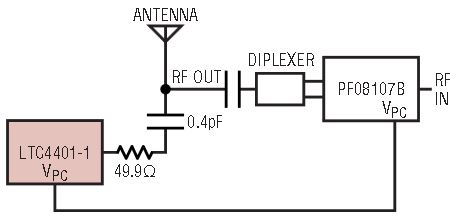
Figure 19. Block diagram of directional coupler alternative.
This new scheme completely eliminates the directional coupler, 50Ω termination resistor, and 68Ω shunt resistor. Instead, the RF signal is fed directly to the diplexer from the power amplifier. The RF signal is coupled back to the LTC4401-1 via a capacitor and a series resistor. The component count is reduced by two.
The series capacitor should be in the range of 0.3pF to 0.4pF and have a tolerance of ±0.05pF or less. The tolerance is important because it directly affects how much RF signal is coupled back to the RF pin on the LTC4400/4401. ATC has ultra-low ESR, high Q microwave capacitors with the tolerances desired. The ATC 600S0R3AW250XT and ATC 600S0R4AW250XT are 0.3pF and 0.4pF capacitors with 0.05pF tolerance. These capacitors come in a small 0603 package. The series resistor is 49.9Ω with 2% tolerance as shown in Figure 19. There are several factors to consider when using this technique, such as board layout and loading in the main line. For example, parasitic effects can significantly alter the feedback network characteristics.
Conclusion
Linear Technology has introduced two new controllers to its RF power controller family. The LTC4400-1 and LTC4401-1 represent small, low power solutions for RF power control. The integration of the RF detector, auto zero system and compensated loop amplifier have produced a temperature stable RF power control solution. External and internal voltage offset changes due to temperature or power supply are cancelled whenever the part cycles through shutdown. These products are available in a small, low profile ThinSOT package and operate over a frequency range of 800MHz to 2700MHz. The demo boards discussed here and ramp-shaping software are available upon request. Demo boards featuring power amplifiers made by Anadigics, Conexant, Hitachi and RFMD are also available.


