High Efficiency 17V, 2A Synchronous Monolithic Step-Down Regulator with Ultralow Quiescent Current in a 3mm × 3mm DFN
High Efficiency 17V, 2A Synchronous Monolithic Step-Down Regulator with Ultralow Quiescent Current in a 3mm × 3mm DFN
2016-02-01
Portable power electronic devices require compact power supplies that can deliver high efficiency over wide input and output voltage ranges. Other requirements include low standby current, low dropout operation, output voltage accuracy and a fast loop response to line and load transient. The LTC3624 is a 17V, 2A synchronous monolithic step-down regulator, featuring ultralow quiescent current and high efficiency over a wide VIN and VOUT range—an excellent choice for battery powered equipment, portable instrumentation, emergency radios and general purpose step-down power supplies.
Some of the LTC3624’s notable features:
- Wide VIN range: 2.7V to 17V
- Wide VOUT range: 0.6V up to VIN at 2A rated output current
- 95% peak efficiency
- Constant frequency of 1MHz or 2.25MHz
- Ultralow quiescent current of 3.5μA
- Low dropout operation at high duty cycle
- Current mode architecture, allowing excellent line and load transient response.
Despite its small size, the LTC3624 remains flexible, enabling designers to optimize solutions by simply selecting a desired mode or frequency of operation. A user-selectable mode input is provided with the following options: Burst Mode operation provides the highest efficiency at light loads, while pulse-skipping mode provides the lowest output voltage ripple. Forced continuous conduction mode is also available for low EMI and to minimize high frequency noise interference. The mode pin can also be used to synchronize the internal system clock to an external clock within ±40% of the nominal switching frequency. The LTC3624 (1MHz) or LTC3624-2 (2.25MHz), is available in a compact 8-lead DFN (3mm × 3mm) thermally enhanced package.
17V, 2A Synchronous Step-Down Regulator
LTC3624 can be optimized to operate over wide VIN and VOUT ranges, using just a few small footprint, low cost external components and a single ceramic output capacitor, as shown in Figure 1. The entire solution fits within a 13mm × 12mm footprint, as shown in Figure 2.
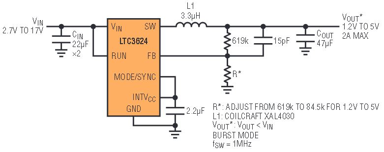
Figure 1. 17V, 2A synchronous step-down regulator featuring the LTC3624.
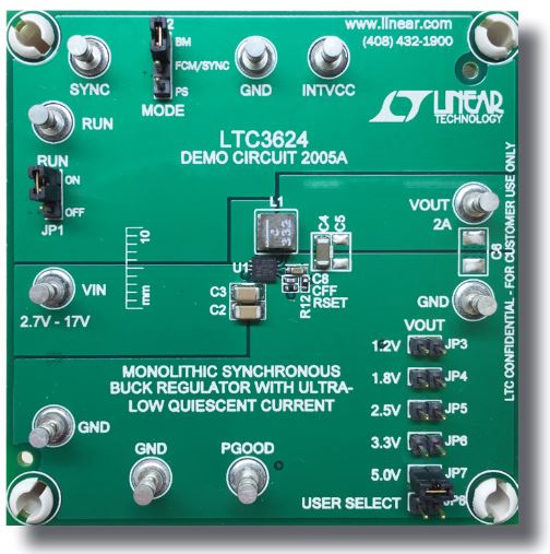
Figure 2. Small total solution size: 13mm × 12mm.
High Efficiency Over a Wide Range of Input and Output Voltages and Loads
The LTC3624 delivers high efficiency over a wide range of input and output voltages, as shown in Figures 3 and 4. Figure 5 shows the light load efficiency. Figure 6 shows the thermal response at 12V input to 5V output, maximum load.

Figure 3. High efficiency is maintained over a wide range of output voltages and loads.
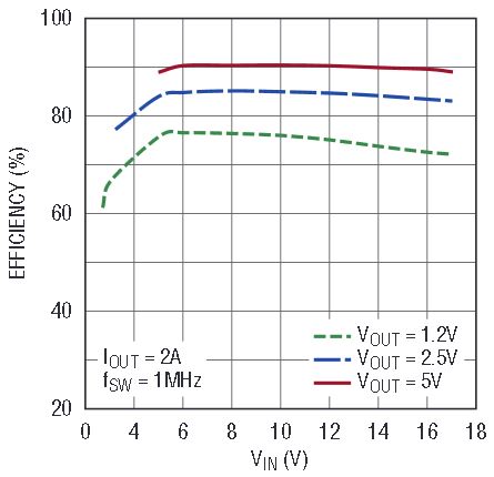
Figure 4. Efficiency also remains high over a wide range of input voltages.
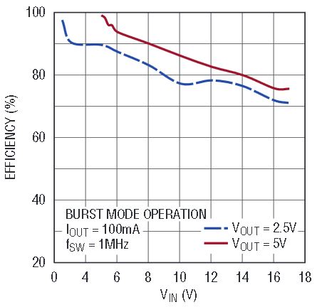
Figure 5. Light load efficiency vs input voltage.
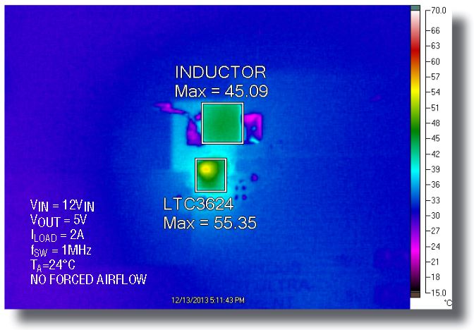
Figure 6. Thermal performance.
Selecting Burst Mode operation yields the highest efficiency at light load, as switching loss is significantly reduced. Furthermore, LTC3624 uses the integrated high side MOSFET’s RDS(ON) as a current sensing element, eliminating the use of an additional sense resistor in the current path, thereby improving overall efficiency.
Fast Load Transient Response
LTC3624 uses a constant frequency, peak current mode control architecture that yields fast loop response to the sudden changes in load current. The load transient response is shown in Figure 7. Using only one ceramic output capacitor in the design, the output voltage spike at 25% load step is well limited within ±4% of VOUT. For duty cycle of 41.6% and a 50% load step, the output voltage spike is less than ±5% as shown in Figure 8.
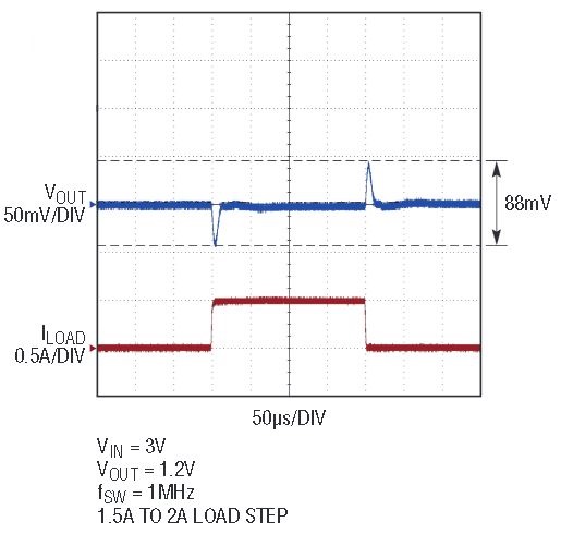
Figure 7. Load step transient response for 3V input, 1.2V output.
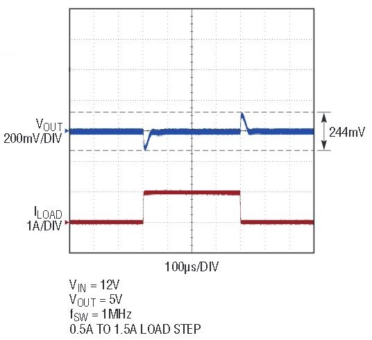
Figure 8. Load step transient response for 12V input, 5V output.
High Duty Cycle/Low Dropout Operation
Due to the increasing demand in battery powered devices operating at high duty cycle while maintaining VOUT within its regulation window, LTC3624 is designed to operate in low dropout mode.
When the input supply voltage is decreasing toward the output voltages and the duty cycle approaches 100%, if FCM mode is selected, the high side MOSFET is turned on continuously and all active circuits are kept alive. The required headroom voltage for VOUT to maintain regulation at full load is determined by VIN minus nominal VOUT, the voltage drop across the high side MOSFET’s RDS(ON) and the output inductor’s parasitic DCR.
If Burst Mode operation or pulse skipping mode is selected, the part transitions in and out of sleep mode depending on the output load current, thus reducing the quiescent current and extending the life of the battery. Figure 5 shows the minimal energy used to maintain the output near dropout and light loads.
Other Features
LTC3624 incorporates other features to keep it functioning properly under fault conditions and allow it to be used in a variety of applications.
Output Overcurrent and VIN Overvoltage Protection
The built-in current limit protects the part from exceeding rated power dissipation if the output is temporarily overloaded. The VIN overvoltage fault limit function protects the internal MOSFET devices from transient voltage spikes. As VIN rises above 19V, the part shuts down both high side and low side MOSFETs and resumes normal operation as VIN drops below 18.5V.
Soft-Start and PGOOD Indicator
An internal 1ms soft-start ramp allows the part to rise smoothly from 0V to its set voltage without a sudden inrush of current. If the output power good signal, PGOOD, is high, the output voltage is within the ±7.5% window of the nominal set voltage, otherwise it stays low. There is a blanking delay of approximate 32 switching cycles to avoid unwanted noise coupled into the PGOOD signal during any disturbance or transient at VOUT.
Frequency Synchronization
Frequency sync capability allows the internal oscillator to be synchronized to an external clock signal applied at MODE/SYNC pin. This is a simple way to program the switching frequency of the part to ±40% of its fixed internal preset frequency.
Conclusion
The LTC3624’s small footprint and high power density in a thermally enhanced package make it an excellent choice for portable electronic devices. The LTC3624 features ultralow quiescent current, high efficiency, low dropout operation, wide VIN and VOUT ranges and embedded protection functions. It is an attractive option for users seeking to improve a system’s overall efficiency, power density and reliability.


