Synchronous Buck Converter Requires Only 1.5V Input
The LTC3713 is a low input voltage, synchronous buck converter capable of operating from a supply voltage as low as 1.5V. The LTC3713 combines a step-down controller with a boost converter all in one package. Both sections operate independently of one another, but can be used together to form an efficient, monolithic, low input voltage, buck switching regulator. The regulator also has the ability to source and sink current, making it suitable for bus termination applications.
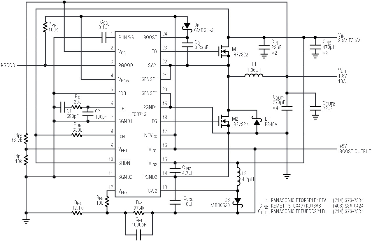
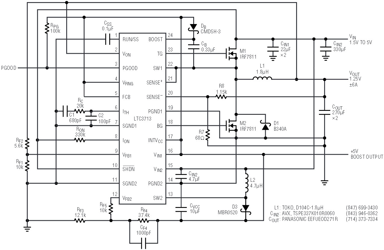
Figure 1 and Figure 2 show two circuits where the boost converter generates a 5V output that powers the top and bottom MOSFET drivers, along with most of the internal circuitry, of the buck controller. This topology precludes the need for low threshold power MOSFETs, because the buck controller section always operates from the boosted 5V output regardless of the input supply voltage. The entire system can remain functional down to an input voltage of 1.5V, the minimum operating voltage of the boost converter section.

Figure 1. 1.8V, 10A buck converter at 300kHz.

Figure 2. 1.8V, 10A buck converter at 300kHz.
The boost regulator portion within the LTC3713 is a current mode, fixed frequency step-up DC/DC converter. The external passive components for the boost converter consist of L2, D3, CVCC, CF4, RF3, RF4, and RF5. The resistor divider, RF3 and RF4, sets the boost output voltage to 5V. The 5V boosted output is connected to the INTVCC and VIN1 pins, allowing the buck regulator section to be powered from the output of the boost converter.
The buck regulator portion within the LTC3713 is a synchronous, current mode step-down controller. It utilizes a valley current control architecture along with MOSFET VDS sensing to deliver very low on-times without a sense resistor. In Figure 1 and Figure 2, RF1 and RF2 form a resistor divider that senses the output voltage and compares it with an internal reference voltage to regulate the output voltage at 1.8V (Figure 1) or 1.25V (Figure 2). Power for the top and bottom MOSFET drivers and most of the internal controller circuitry is derived from the INTVCC pin. The top MOSFET driver is powered from a floating bootstrap capacitor that is recharged from INTVCC through an external Schottky diode when the top MOSFET is turned off. Inductor current is determined by sensing the voltage between the SENSE+ and SENSE– pins using the bottom MOSFET on-resistance. If a better defined current limit is required, the SENSE+ and SENSE– pins could be connected across a sense resistor placed between the source of the bottom MOSFET and ground. The voltage on the ITH pin sets the inductor valley current and adjusts it to match the load current.
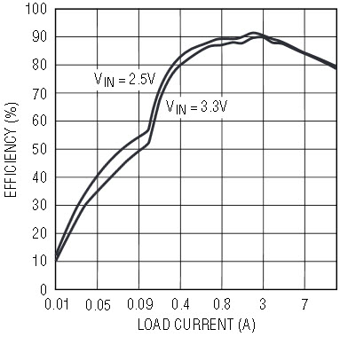
Figure 1 illustrates a design solution for an application requiring an output voltage of 1.8V, with 10A of load current, from an input voltage in the range of 2.5V to 5V. Figure 3 shows efficiency for this circuit at input voltages of 2.5V and 3.3V. Because this circuit only sources current, the SENSE– pin is connected directly to the source of the bottom MOSFET.

Figure 3. Efficiency vs load current for the circuit in Figure 1.
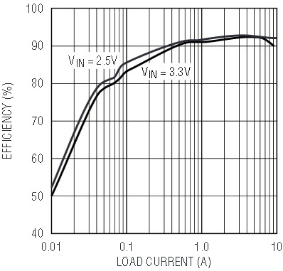
The LTC3713 can also be used in applications in which the output will be sourcing and sinking current. Figure 2 shows a circuit with an output voltage of 1.25V that can source and sink 6A from an input voltage in the range of 1.5V to 5V. R7 and R8 are used to introduce a 70mV offset voltage into the sense voltage that allows the LTC3713 to source and sink a symmetrical amount of load current. Figure 4 shows efficiencies for this circuit at input voltages of 2.5V and 3.3V.

Figure 4. Efficiency vs load current for the circuit in Figure 2
In summary, the LTC3713 provides a complete solution for applications that require a step-down conversion from a low input voltage. The onboard boost converter makes this possible while still achieving high efficiencies.


