A Standards Lab Grade 20-Bit DAC with 0.1ppm/°C Drift
Introduction
Significant progress in high precision, instrumentation grade D-to-A conversion has recently occurred. Ten years ago 12-bit D-to-A converters (DACs) were considered premium devices. Today, 16-bit DACs are available and increasingly common in system design. These are true precision devices with less than 1LSB linearity error and 1ppm/°C drift. Nonetheless, there are DAC applications that require even higher performance. Automatic test equipment, instruments, calibration apparatus, laser trimmers, medical electronics and other applications often require DAC accuracy beyond 16 bits. 18-bit DACs have been produced in circuit assembly form, although they are expensive and require frequent calibration. 20 and even 23+ (0.1ppm!) bit DACs are represented by manually switched Kelvin-Varley dividers. These devices, although amazingly accurate, are large, slow and extremely costly. Their use is normally restricted to standards labs. A useful development would be a practical, 20-bit (1ppm) DAC that is easily constructed and does not require frequent calibration.1
20-Bit DAC Architecture
Figure 1 diagrams the architecture of a 20-bit (1ppm) DAC. This scheme is based on the availability of a true 1ppm analog-to-digital converter with scale and zero drifts below 0.02ppm/°C. This device, the LTC2400, is used as a feedback element in a digitally corrected loop to realize a 20-bit DAC.

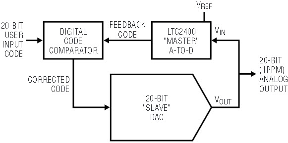
Figure 1. Conceptual, loop-based 20-bit DAC: digital comparison allows A-to-D to correct DAC errors. The LTC2400 A-to-D’s low uncertainty characteristics permit 1ppm output accuracy.
In practice, the “slave” 20-bit DAC’s output is monitored by the “master” LTC2400 A-to-D, which feeds digital information to a code comparator. The code comparator differences the user input word with the LTC2400 output, presenting a corrected code to the slave DAC. In this fashion, the slave DAC’s drifts and nonlinearity are continuously corrected by the loop to an accuracy determined by the A-to-D converter and VREF.2 No other components in the loop need to be stable.
This loop has a number of desirable attributes. As mentioned, accuracy limitations are set by the A-to-D converter and its reference. Additionally, loop behavior averages low order bit indexing and jitter, obviating the loop’s inherent small-signal instability. Finally, classical remote sensing may be used or digitally based sensing is possible by placing the A-to-D converter at the load. The A-to-D’s SO-8 package and lack of external components makes this digitally incarnated Kelvin sensing scheme practical.3
Circuitry Details
Figure 2 is a detailed schematic of the 1ppm DAC. The slave DAC comprises two DACs. The upper 16 bits of the code comparator’s output are fed to a 16-bit DAC (“MSB DAC”), while the lower bits are converted by a separate DAC (“LSB DAC”). Although a total of 32 bits are presented to the two DACs, there are 8 bits of overlap, ensuring loop capture under all conditions. The composite DACs’ resultant 24-bit resolution provides 4 bits of indexing range below the 20th bit, ensuring a stable LSB of 1ppm of scale. A1 and A2 transform the DAC’s output currents into voltages, which are summed at A3. A3’s scaling is arranged so that the correction loop can always capture and correct any combination of zero- and full-scale errors. A3’s output, the circuit output, feeds the LTC2400 A-to-D. The LT1010 provides buffering to drive loads and cables. The A-to-D’s digital output is differenced against the input word by the code comparator, which produces a corrected code. This corrected code is applied to the MSB and LSB DACs, closing a feedback loop. The loop’s integrity is determined by A-to-D converter and voltage reference errors. The resistor and diodes at the 5V powered A-to-D protect it from inadvertent A3 outputs (power up, transient, lost supply, etc.). A4 is a reference inverter and A5 provides a clean ground potential to both DACs.

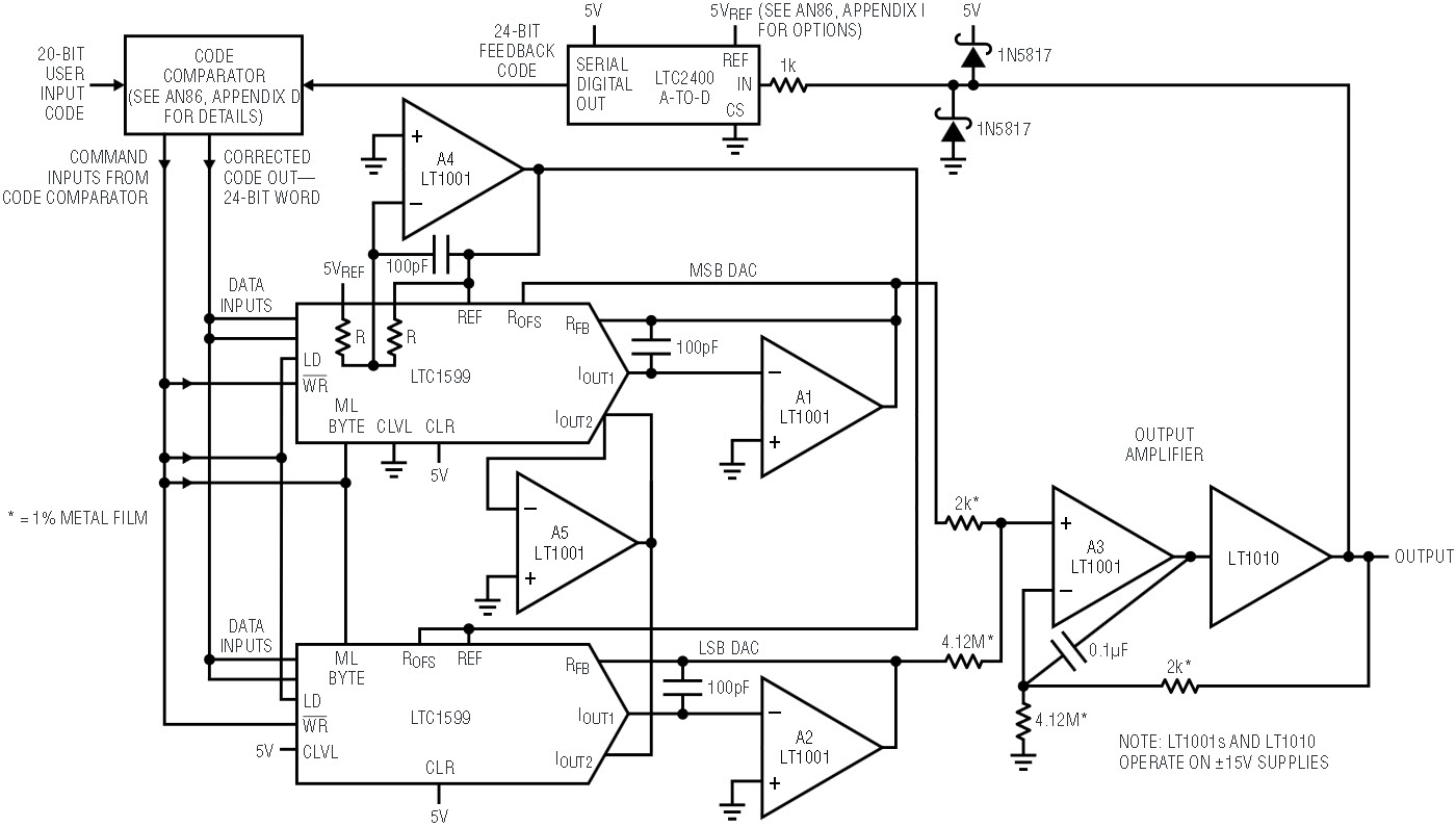
Figure 2. Detail of 1ppm DAC: composite DAC comprises two DAC values summed at the output amplifier. The LTC2400 A-to-D and code comparator furnish stabilizing feedback.
Linearity Considerations
A-to-D linearity determines overall DAC linearity. The A-to-D has about ±2ppm nonlinearity. In applications where this error is permissible, it may be ignored. If 1ppm linearity is required, it is obtainable by correcting the residual linearity error with software techniques. Details on LTC2400 linearity and this feature are presented in Appendices D and E of AN86.
DC Performance Characteristics
Figure 3 is a plot of linearity vs input code. The data shows linearity is within 1ppm over all codes. Output noise, measured in a 0.1Hz to 10Hz bandpass, is seen in Figure 4 to be about 0.2LSB. This measurement is somewhat corrupted by equipment limitations, which set a noise floor of about 0.2µV.

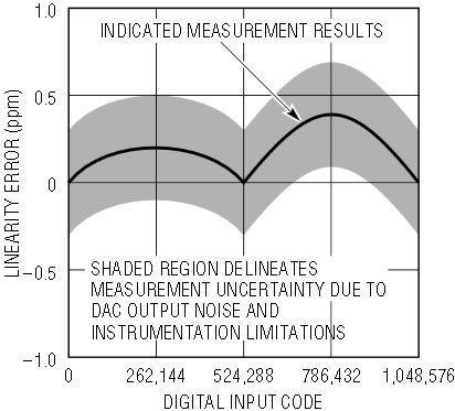
Figure 3. Linearity plot shows no error outside 1ppm for all codes.

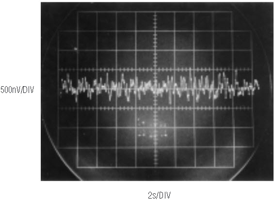
Figure 4. Output noise indicates less than 1µV, about 0.2LSB. The measurement noise floor, due to equipment limitations, is 0.2µV.
Dynamic Performance
The A-to-D’s conversion rate combines with the loop’s sampled data characteristic and slow amplifiers to dictate relatively slow DAC response. Figure 5’s slew response requires about 150 microseconds.

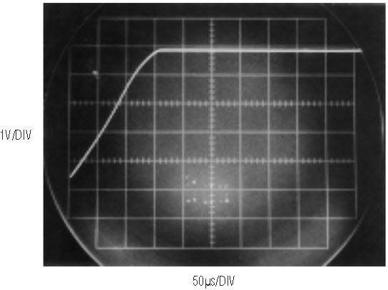
Figure 5. DAC output full-scale slew characteristics.
Figure 6 shows full-scale DAC settling time to within 1ppm (±5µV) requires about 1400 milliseconds. A smaller step (Figure 7) of 500µV needs only 100 milliseconds to settle within 1ppm.

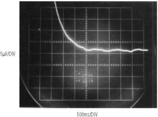
Figure 6. High resolution settling detail after a full-scale step: settling time is 1400 milliseconds to within 1ppm (±5µV).

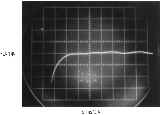
Figure 7. Small-step settling time measures 100 milliseconds to within 1ppm (±5µV) for a 500µV transition.
Conclusion
Summarized 1ppm DAC specifications appear in Table 1. These specifications should be considered guidelines, as the options and variations noted will affect performance. Consult the appropriate appendices of LTC Application Note 86 for design specifics and trade-offs.
| Parameter | Specification |
| Resolution | 1ppm |
| Full-Scale Error | 4ppm of VREF (Trimmable to 1ppm by VREF Adjustment) |
| Full-Scale Error Drift | 0.04ppm/° C Exclusive of Reference (0.1ppm/° C with LTZ1000A Reference) See Note 4 |
| Offset Error | 0.5ppm |
| Offset Error Drift | 0.01ppm/° C |
| Nonlinearity | ±2ppm, Trimmable to Less Than 1ppm See Note 5 |
| Output Noise | 0.2ppm (≈0.9μV, 0.1Hz to 10Hz BW) |
| Slew Rate | 0.033V/μs |
| Settling Time—Full-Scale Step | 1400 Milliseconds |
| Settling Time—500μV Step | 100 Milliseconds |
| Output Voltage Range | 0V to 5V. For Other Ranges See Note 6 |
| Note 4: See AN 86, Appendix I Note 5: See AN 86, Appendix E Note 6: See AN 86, Appendices E and F |
|
1 This article is excerpted from Linear Technology Application Note 86, A Standards Lab Grade 20-Bit DAC with 0.1ppm/°C Drift. Considerably more detail is available in that publication.
2 D-to-A converters have been placed in loops to make A-to-D converters for a long time. Here, an A-to-D converter feeds back a loop to form a D-to-A converter. There seems a certain justified symmetry to this development. Turnabout is indeed fair play.
3 One wonders what Lord Kelvin’s response would be to the digitization of his progeny. Such uncertainties are the residue of progress.
关于作者


