A 4.5ns, 4mA, Single-Supply, Dual Comparator Optimized for 3V/5V Operation
A 4.5ns, 4mA, Single-Supply, Dual Comparator Optimized for 3V/5V Operation
1998-11-01
Introduction
The LT1720 is an UltraFast™ (4.5ns), low power 4mA/comparator), single-supply, dual comparator designed to operate on a single 3V or 5V supply. These comparators feature internal hysteresis, making them easy to use, even with slowly moving input signals. The LT1720 is fabricated in Analog Devices' 6GHz complementary bipolar process, resulting in unprecedented speed for its low power consumption. Table 1 summarizes the LT1720’s performance specifications.
| Parameter | Conditions | Value |
| Propagation Delay | Overdrive = 20mV | 4.5ns |
| Propagation Delay | Overdrive = 5mV | 7ns |
| Supply Current | VCC = 5V | 4mA per Comparator |
| Supply Voltage | Full Temperature Range Limits | 2.7V to 6V |
| input Voltage Range | Full Temperature Range Limits | –0.1V to ( VCC – 1.2V) |
| Input Offset Voltage | VCC = 5V, VCM = 1V | 1mV |
| Input-Referred Hysteresis | VCC = 5V, VCM = 1V | 3.5mV |
| Output Voltage (Low) | ISINK = 10mA | 0.4V Max |
| Output Voltage (High) | ISOURCE = 4mA | (VCC – 0.4V) Min |
The LT1720 is offered in SO-8, with just three pins per comparator plus power and ground. For a full-featured, 7ns, single-supply comparator with dual complementary outputs and internal latch, the LT1394 is available from this same high speed process.
These fast, small, low power comparators are versatile building blocks for a variety of high speed, single-supply applications, such as clock generators, window comparators, timing skew generators, coincidence detectors and pulse stretchers.
Circuit Description
The block diagram of one comparator in the LT1720 is shown in Figure 1. There are differential inputs (+IN/ –IN), an output (OUT), a single positive supply (VCC) and ground (GND). The two comparators are completely independent, sharing only the power and ground pins. The circuit topology consists of a differential input stage, a gain stage with hysteresis and a complementary common-emitter output stage. All of the internal signal paths utilize low voltage swings for high speed at low power.

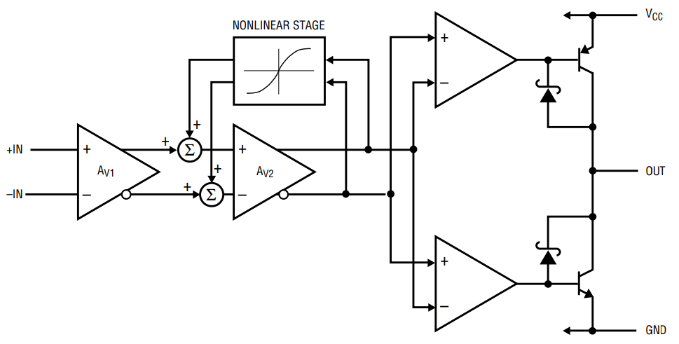
Figure 1. LT1720 block diagram.
The input stage topology maximizes the input dynamic range available without requiring the power, complexity and die area of two complete input stages such as are found in rail-to-rail input comparators. With a 2.7V supply, the LT1720 still has a respectable 1.6V of input common mode range. The differential input voltage range is rail-to-rail, without the large input currents found in competing devices. The input stage also features phase reversal protection to prevent false outputs when the inputs are driven below the –100mV common mode voltage limit.
The internal hysteresis is implemented by positive, nonlinear feedback around a second gain stage. Until this point, the signal path has been entirely differential. The signal path is then split into two drive signals for the upper and lower output transistors. The output transistors are connected common emitter for rail-to-rail output operation. The Schottky clamps limit the output voltages at about 300mV from the rail, not quite the 50mV or 15mV of Analog Devices' rail-to-rail amplifiers and other products. But the output of a comparator is digital, and this output stage can drive TTL or CMOS directly. It can also drive a host of other loads, as will be demonstrated in the applications below.
The bias conditions and signal swings in the output stages are designed to turn their respective output transistors off faster than on. This nearly eliminates the surge of current from VCC to ground that occurs at transitions, keeping the power consumption low even with high output-toggle frequencies. In fact, the internal-frequency-dependent current drain is the equivalent of putting just 15pF on the output. The low surge current also helps keep the LT1720 well behaved in high speed applications.
Internal Hysteresis
The LT1720 includes internal hysteresis, eliminating the linear region where high speed comparators are most temperamental. The input-output transfer characteristic is illustrated in Figure 2, which shows the definitions of VOS and VHYST based upon the two measurable trip points. The 3.5mV (typical) hysteresis band makes the LT1720 well behaved, even with slowly moving inputs.

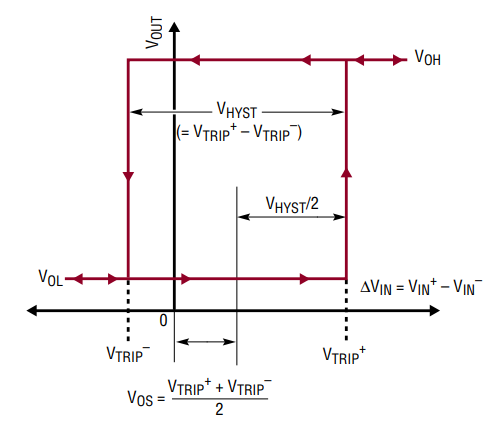
Figure 2. Hysteresis I/O characteristics.
The exact amount of hysteresis will vary from unit-to-unit; the LT1720 specifications include both upper and lower limits that are guaranteed over temperature. The hysteresis will also vary slightly with changes in supply voltage and common mode voltage. If a comparator is used to detect a threshold crossing in one direction only, only that trip point is significant. Therefore, a stable offset voltage with an unpredictable level of hysteresis, as seen in many competing comparators, is useless. The LT1720 is many times better than prior comparators in this regard. Figure 3 shows a typical LT1720’s input voltages vs supply voltages. The VOS shift is only 320µV, corresponding to a typical PSRR of 80dB.

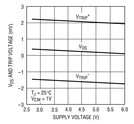
Figure 3. The LT1720’s hysteresis is insensitive to supply-voltage variations.
Speed Limits
The LT1720 comparators are intended for high speed applications, where it is important to understand a few limitations. These limitations can roughly be divided into three categories: input speed limits, output speed limits and internal speed limits.
There are no significant input speed limits except the shunt capacitance of the input nodes. If the 2pF typical input nodes are driven, the LT1720 will respond.
The output speed is constrained by the slew currents available from the output transistors. To maintain low power quiescent operation, the LT1720 output transistors are sized to deliver 25mA–45mA typical slew currents. This is sufficient to drive small capacitive loads and logic gate inputs at extremely high speeds. But the slew rate will slow dramatically with heavy capacitive loads. Because the propagation delay (tPD) definition ends at the time the output voltage is halfway between the supplies, the fixed slew current actually makes the LT1720 faster at 3V than 5V with 20mV of input overdrive.
The internal speed limits manifest themselves as dispersion. All comparators have some degree of dispersion, defined as a change in propagation delay vs input overdrive. The propagation delay of the LT1720 will vary with overdrive, from a typical of 4.5ns at 20mV overdrive to 7ns at 5mV overdrive (typical). The LT1720’s primary source of dispersion is the hysteresis stage. As a change of polarity arrives at the gain stage, the positive feedback of the hysteresis stage subtracts from the overdrive available. Only when enough time has elapsed for a signal to propagate forward through the gain stage, backwards through the hysteresis stage and forward through the gain stage again, will the output stage receive the same level of overdrive that it would have received in the absence of hysteresis.
With 5mV of overdrive, the LT1720 is faster with a 5V supply than with a 3V supply, the opposite of what is true with 20mV overdrive. This is due to the internal speed limit, because the gain stage is faster at 5V than 3V due primarily to the reduced junction capacitances with higher reverse voltage bias.
In many applications, as shown in the following examples, there is plenty of input overdrive. Even in applications providing low levels of overdrive, the LT1720 is fast enough that the absolute dispersion of 2.5ns (= 7 – 4.5) is small enough to ignore.
The gain and hysteresis stage of the LT1720 is simple, short and high speed to minimize dispersion. This internal “self-latch” can be usefully exploited in many applications because it occurs early in the signal chain, in a low power, fully differential stage. It is therefore highly immune to disturbances from other parts of the circuit, either in the same comparator, on the supply lines or from the other comparator in the same package. Once a high speed signal trips the hysteresis, the output will respond, after a fixed propagation delay, without regard to these external influences that can cause trouble in nonhysteretic comparators.
Applications
Crystal Oscillators
Figure 4 shows a simple crystal oscillator using one half of an LT1720. The 2k–620Ω resistor pair set a bias point at the comparator’s noninverting input. The 2k–1.8k–0.1µF path sets the inverting input node at an appropriate DC average level based on the output. The crystal’s path provides resonant positive feedback and stable oscillation occurs. Although the LT1720 will give the correct logic output when one input is outside the common mode range, additional delays may occur when it is so operated, opening the possibility of spurious operating modes. Therefore, the DC bias voltages at the inputs are set near the center of the LT1720’s common mode range and the 220Ω resistor attenuates the feedback to the noninverting input. The circuit will operate with any AT-cut crystal from 1MHz to 10MHz over a 2.7V to 6V supply range.

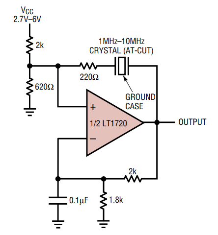
Figure 4. Simple 1MHz–10MHz crystal oscillator.
The output duty cycle for the circuit of Figure 4 is roughly 50% but it is affected by resistor tolerances and, to a lesser extent, by comparator offsets and timings.
The circuit of Figure 5 creates a pair of complementary outputs with a forced 50% duty cycle. Crystals are narrow-band elements, so the feedback to the noninverting input is a filtered analog version of the square wave output. Changing the noninverting reference level can therefore vary the duty cycle. C1 operates as in the previous example, whereas C2 creates a complementary output by comparing the same two nodes with the opposite input polarity. A1 compares band-limited versions of the outputs and biases C1’s negative input. C1’s only degree of freedom to respond is variation of pulse width; hence the outputs are forced to 50% duty cycle. This circuit works well because of the two matched delays and rail-to-rail style outputs.

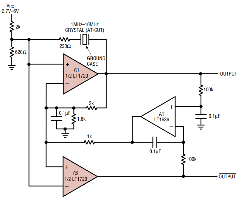
Figure 5. Crystal oscillator with complementary outputs and 50% duty cycle.
The circuit in Figure 6 shows a crystal oscillator circuit that generates two nonoverlapping clocks by making full use of the two independent comparators of the LT1720. C1 oscillates as before, but with a lower reference level, C2’s output will toggle at different times. The resistors set the degree of separation between the output’s high pulses. With the values shown, each output has a 44% high and 56% low duty cycle, sufficient to allow 2ns between the high pulses where both are at logic low. Figure 7 shows the two outputs.

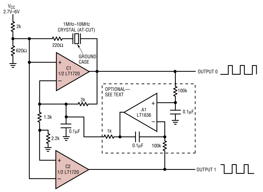
Figure 6. Crystal-based nonoverlapping 10MHz clock generator.

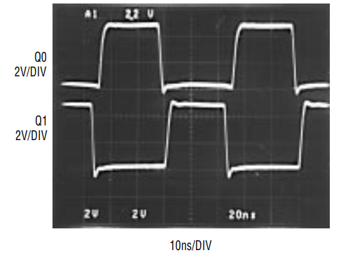
Figure 7, Nonoverlapping outputs of Figure 6’s circuit.
The optional A1 feedback network shown can be used to force identical output duty. Because the reference level set for C2 is lower than that set for C1, the steady state duty cycles will be 44% rather than 50%. Note, though, that the addition of this network only adjusts the percentage of time each output is high to be the same, which can be important in switching circuits requiring identical settling times. It cannot adjust the relative phases between the two outputs to be exactly 180° apart because the signal at the input node driven by the crystal is not an exact sinusoid.
Timing Skews
For a number of reasons, the LT1720 is an excellent choice for applications requiring differential timing skew. The two comparators in a single package are inherently well matched, with just 300ps ∆tPD typical. Monolithic construction keeps the delays well matched vs supply voltage and temperature. Crosstalk between the comparators, usually a disadvantage in monolithic duals, has minimal effect on the LT1720 timing due to the internal hysteresis, as discussed earlier.
The circuits of Figure 8 show basic building blocks for differential timing skews. The 2.5k resistance interacts with the 2pF typical input capacitance to create at least ±4ns delay, controlled by the potentiometer setting. A differential and a single-ended version are shown. In the differential configuration, the output edges can be smoothly scrolled through ∆t = 0 with negligible interaction.

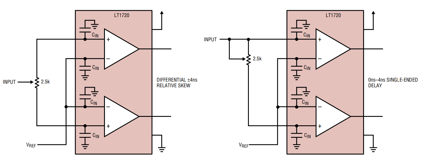
Figure 8. Timing-skew generation is easy with the LT1720.
Fast Waveform Sampler
Figure 9 uses a diode-bridge-type switch for clean, fast waveform sampling. The diode bridge, because of its inherent symmetry, provides lower AC errors than other semiconductor-based switching technologies. This circuit features 20dB of gain, 10MHz full power bandwidth and 100µV/°C baseline uncertainty. Switching delay is less than 15ns and the minimum sampling window width for full power response is 30ns.

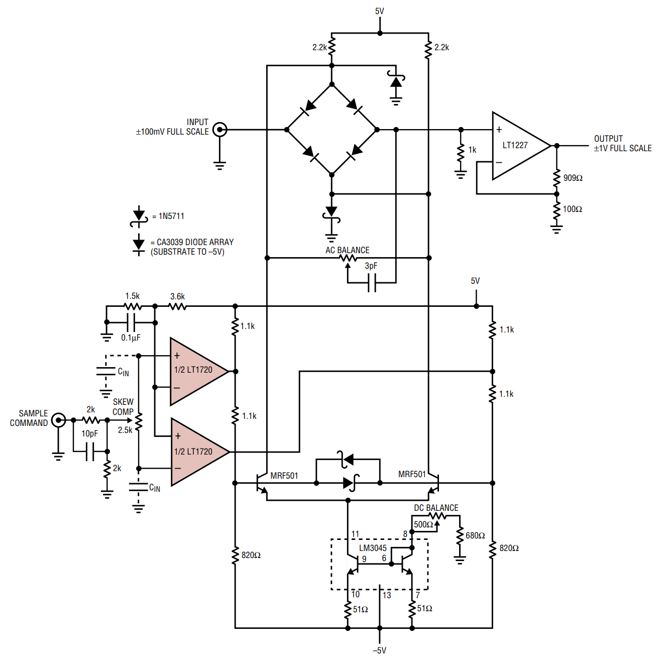
Figure 9. Fast waveform sampler using the LT1720 for timing-skew compensation.
The input waveform is presented to the diode bridge switch, the output of which feeds the LT1227 wideband amplifier. The LT1720 comparators, triggered by the sample command, generate phase-opposed outputs. These signals are level shifted by the transistors, providing complementary bipolar drive to switch the bridge. A skew compensation trim ensures bridge-drive signal simultaneity within 1ns. The AC balance corrects for parasitic capacitive bridge imbalances. A DC balance adjustment trims bridge offset.
The trim sequence involves grounding the input via 50Ω and applying a 100kHz sample command. The DC balance is adjusted for minimal bridge ON vs OFF variation at the output. The skew compensation and AC balance adjustments are then optimized for minimum AC disturbance in the output. Finally, unground the input and the circuit is ready for use.
Coincidence Detector
High speed comparators are especially suited for interfacing pulse-output transducers, such as particle detectors, to logic circuitry. The matched delays of a monolithic dual are well suited for those cases where the coincidence of two pulses needs to be detected. The circuit of Figure 10 is a coincidence detector that uses an LT1720 and discrete components as a fast AND gate.

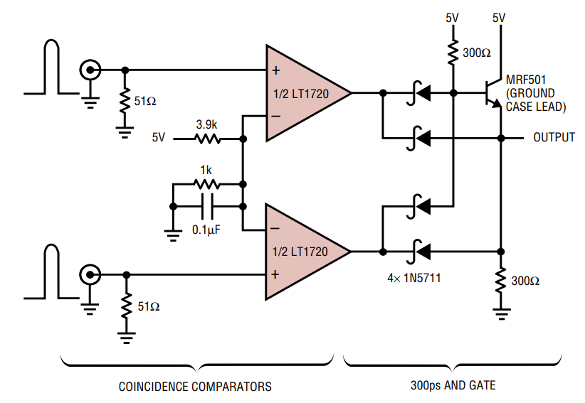
Figure 10. A 2.5ns coincidence detector.
The reference level is set to 1V, an arbitrary threshold. Only when both input signals exceed this will a coincidence be detected. The Schottky diodes from the comparator outputs to the base of the MRF-501 form the AND gate, while the other two Schottkys provide for fast turn-off. A logic AND gate could instead be used, but would add considerably more delay than the 300psec contributed by this discrete stage.
This circuit can detect coincident pulses as narrow as 2.5ns. For narrower pulses, the output will degrade gracefully, responding, but with narrow pulses that don’t rise all the way to high before starting to fall. The decision delay is 4.5ns with input signals 50mV or more above the reference level. This circuit creates a TTL compatible output but it can typically drive CMOS as well.
Pulse Stretcher
For detecting short pulses from a single sensor, a pulse stretcher is often required. The circuit of Figure 11 acts as a one-shot, stretching the width of an incoming pulse to a consistent 100ns. Unlike a logic one-shot, this LT1720-based circuit requires only 100pV-s of stimulus to trigger.

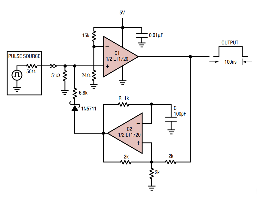
Figure 11. A 1ns pulse stretcher.
The circuit works as follows: Comparator C1 functions as a threshold-detector, whereas comparator C2 is configured as a one-shot. The first comparator is prebiased with a threshold of 8mV to overcome comparator and system offsets and establish a low output in the absence of an input signal. An input pulse sends the output of C1 high, which in turn latches C2’s output high. The output of C2 is fed back to the input of the first comparator, causing regeneration and latching both outputs high. Timing capacitor C now begins charging through R and, at the end of 100ns, C2 resets low. The output of C1 also goes low, latching both outputs low. A new pulse at the input of C1 can now restart the process. Timing capacitor C can be increased without limit for longer output pulses.
This circuit has an ultimate sensitivity of better than 14mV with 5ns–10ns input pulses. It can even detect an avalanche generated test pulse of just 1ns duration with sensitivity better than 100mV.1 It can detect short events better than the coincidence detector above because the one-shot is configured to catch just 100mV of upward movement from C1’s VOL, whereas the coincidence detector’s 2.5ns specification is based on a full, legitimate logic high.
Conclusion
The new LT1720 dual 4.5ns single-supply comparators feature high speeds and low power consumption. They are versatile and easy-to-use building blocks for a wide variety of system design challenges.
1 See Analog Devices Application Note 47, Appendix B. This circuit can detect the output of the pulse generator described after 40dB of attenuation.
关于作者


