
Simple Sequencing Circuit
Key Takeaways
|
Abstract
This article explains the sequencing needs of different digital loads and discusses different possibilities for the implementation of a sequencing and voltage monitoring function. A novel, simple-to-use sequencing option is introduced that does not require any programming, digital communication, or bias power supply. These are important features since the sequencer needs to be powered first in a system. By that time, digital devices, which could communicate with the sequencer, usually are not running yet.
Introduction
Electrical loads, such as field programmable gate arrays (FPGAs), graphics processor units (GPUs), and central processing units (CPUs), as well as digital signal processing (DSP) and systems on a chip (SoCs), require sequencing—for example, a predefined order of increase and decrease of the different supply voltages. If the appropriate sequencing is not followed, the function of the load may be limited and defective. Also, in extreme cases the load can be destroyed. To prevent this, sequencing functions are used.
Sequencing Examples
In general, a circuit can also be used in which the different voltage converters switch on one after the other by linking the generated voltages with enable pins. However, this requires voltage converters with an exact definition of the precision enable pin, and a fixed sequence of switch-off of the individual voltages is difficult to implement. Also, the exact time course can only be implemented with cumbersome additional circuitry. This is why a dedicated sequencing controller is often preferred. Figure 1 shows the basic structure of such a system. The voltage converters DCDC1 to DCDC n are switched on and off by a sequencer through the respective enable pins in the correct order.
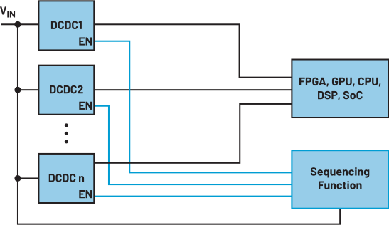
This sequencing device should have a wide, universal input voltage range if possible. It must perform its function before the respective voltages in the system are switched on. Thus, it is favorable if its input voltage range is large.
The sequencing function can consist of different building blocks. For example, a microcontroller, a small and simple FPGA, a special sequencer with programmable memory, or a simple sequencer can be used.
Many of these solutions have unfavorable limitations. A microcontroller must first be in operation and a programmed function must be loaded. A small control FPGA and a sequencer with programmable memory must be programmed before operation. This can be done before the device is soldered onto the board, or it can be done in the soldered state on the board, before the first switch-on. Both can cause considerable effort and costs.
Sequencing Solution
Thus, a solution was developed that does not require programming in production. This is a sequencing solution in which only resistors and capacitors are used to adjust the behavior. Also, this sequencer, with a very wide input voltage range of 2.7V to 15V, can be operated directly from a 3.3V, 5V, or even 12V supply voltage without needing an additional power supply for the sequencer itself.
In Figure 2, in addition to the sequencer task, another helpful function is implemented. The different voltages V1 to V8 are monitored individually. Only when all voltages have reached a predetermined value, a power OK signal is given. The accuracy of this voltage monitoring is important. Monitoring accuracy is a part of the overall accuracy of each voltage generated by a DC-to-DC converter. The ADM6840 has a voltage monitoring accuracy of ±0.8%.
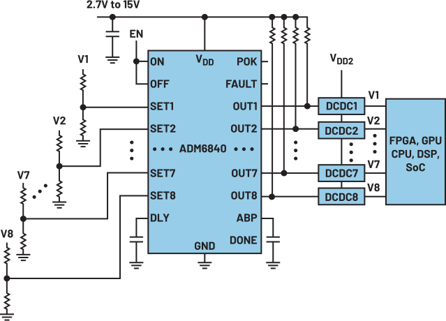
It is essential that a monitoring module works reliably so that a circuit is well protected. Since many circuits can also get quite hot, an ADM6840 can be operated in a temperature range between –40°C and +125°C. If more than eight channels are needed, several sequencers can be operated together.
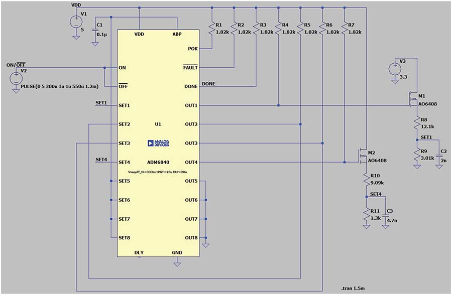
To easily evaluate the function of the ADM6840 sequencer, LTspice® (a free simulation software tool) is available. Within LTspice, the sequencer is available in an example circuit. Figure 3 shows the simulation environment in which different setups can be simulated.
Conclusion
Sequencing can be carried out quite easily with the right building blocks. In most applications, no additional auxiliary power supply is required and there is no need for time-consuming programming. Thus, reliable sequencing can be designed in the shortest possible time.