Simple Logic Provides Sensible Power Control of LT1794-Based ADSL Line Drivers
Simple Logic Provides Sensible Power Control of LT1794-Based ADSL Line Drivers
by
Tim Regan
2001-05-01
Introduction
As the popularity of DSL for high speed Internet access grows, so too does the need for more central office DSL lines to handle the demand. Without the luxury of unlimited space, central office cabinets are filled with racks of circuit cards with each card containing as many as 128 separate DSL ports. At full transmission power, each typical port consumes approximately 1.3 watts and dissipate on the order of 1 watt of power. Should it ever occur that every port in a single cabinet is called into action at the same time, the demand on the power supplies and heat management system would be immense. Fortunately, this is a very rare situation.
The randomness of connections through the central office provides the opportunity for optimizing the overall power consumption of the entire system by reducing the quiescent power consumption of lines that are not in use. This preserves the power available for meeting the actual demand at any point in time. The LT1794 is a 200MHz gain-bandwidth product, 500mA output drive, dual power amplifier optimized for use in central-office DSL line-driving applications. The amplifier’s operating current can be programmed to optimize power consumption. Using one or two I/O lines from the port-controlling DSP device and a few carefully selected resistors, the line driver can be set to operate at any desired quiescent power level in response to intelligent monitoring of the overall system power demands.
The LT1794 Line Driver
Figure 1 illustrates a standard central office ADSL line driver. The LT1794 has been designed to provide sufficient output voltage swing headroom to prevent clipping of the large transient voltages that occur in the complex discrete-multitone (DMT) transmit signal with power supply rails of ±12V or less. Operating each line driver with minimum power supply rails is the best way to reduce the overall power consumption of the system. The next degree of freedom in reducing power consumption is to set the driver operating current to the minimum amount required. The acceptable level is generally determined by testing a complete data transmission loop through worst-case phone line conditions and backing off the driver quiescent current until the data rate or the bit error rate of the transmission just meets the expected performance. For the LT1794, this operating current typically falls in the range of 6mA to 10mA per amplifier, depending on the specific application. Too low an operating current can result in distortion-induced transmission errors, whereas too high an operating current wastes power. The significance of this seemingly small range of current becomes apparent when the power consumption of an entire card is considered. With ±12V power supplies, the idle state power of each driver could range from 144mW to 240mW. Using a 128-port card as an extreme example, the current optimization process could save as much as 12.3 watts of quiescent power consumption.
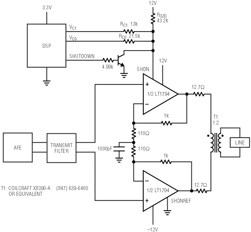
Figure 1. Logic inputs for power control can tailor the power consumption of a standard ADSL line driver.
Two pins of the LT1794 are used to set the operating current: Shutdown (SHDN) and Shutdown Reference (SHDNREF). Figure 2 illustrates the internal biasing circuitry used to program the operating current. In a basic application, a single resistor is selected to fix the operating current of the two current sources. One of these internal current sources provides current to the device start-up circuitry, while the other is scaled up and used to provide bias current to the stages of each amplifier. If the SHDN pin is taken to a voltage within 0.4V of the potential on the SHDNREF pin, the amplifiers are shut off completely and the supply current drops to typically only 100µA. The ultimate power saving approach is to completely shut down idle channels. The optional external transistor shown in Figure 1 or an open-drain logic output can provide the complete shutdown function. The LT1794 wakes up and returns to full operation in just a few microseconds when enabled. One problem with complete shutdown of the driver, however, is that the output stages become very high impedance. In many DSL applications, an idle channel must still remain capable of receiving signals from the line, which are sensed across the transformer back-termination resistors. To receive a signal, the amplifier connection to these resistors cannot be allowed to float.
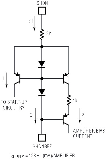
Figure 2. LT1794 internal bias circuitry that sets the operating current.
Three Approaches to Current Control
Fixing the operating current of the LT1794 to the optimum level is a simple matter of selecting a single resistor value. As shown in Figure 3, this can be done in one of two ways. A resistor can be connected between the SHDN pin and the VCC supply of the driver with the SHDNREF pin grounded. Alternately, the SHDN pin can be tied directly to the VCC supply of the driver with a resistor placed between the SHDNREF pin and ground. The design equations are provided in the figure. The only difference between the two approaches is the internal scaling of the programmed current. The power supplies will always provide this current, regardless of whether the driver is actively transmitting data or idle.
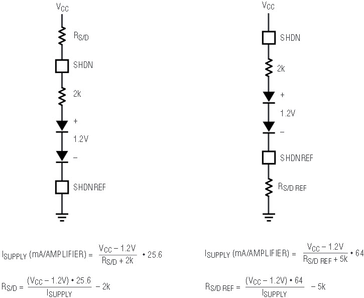
Figure 3. Set it and forget it: single-resistor programming choices.
The two series diode drops (typically 1.2V at 25°C) in the biasing network have a temperature coefficient of approximately –4mV/°C. This causes the operating current to decrease at cold temperatures, with a possibility of dropping below the level required for the desired data transmission performance of the line. In actual systems, the drivers run fairly hot, so this is not normally a problem. If very cold ambient conditions are expected, the operating current should be increased a little to accommodate any change with temperature.
The approach shown in Figure 4 provides the means for a single logic-control bit to reduce the quiescent current to a lower level when the line is idle. A second resistor programs any lower current level desired. This is very useful for power management when the port must remain terminated to receive signals from the line. For the LT1794, with an operating current of only 2mA/amplifier, the output impedance of each amplifier is less than 2Ω up to 1MHz. This partially shutdown state of the line driver keeps the transformer termination resistors connected and able to develop a received signal.
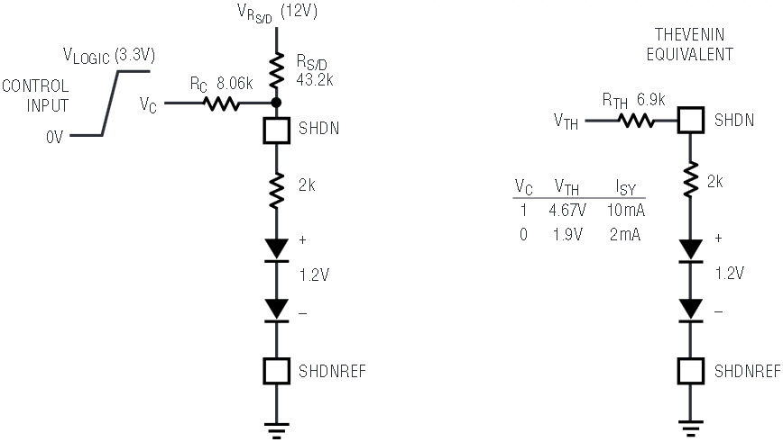
Figure 4. Obtain two operating levels from one logic-control input: the driver can be powered down when idle, but still provides termination for the receive channel.
The control-logic output line sources extra current into the SHDN pin when it is high and the driver is to be operational. When low, the control line takes away from the available current to the SHDN pin. Proper selection of the resistor values can be a little tricky because the voltage at the shutdown pin changes as the current into it varies. The Thevenin-equivalent circuit, also shown in Figure 4, is an easy way to evaluate the circuit operation. The single Thevenin resistance, RTH, is the parallel combination of the RS/D resistor and the logic control resistor, RC. The RS/D resistor is normally connected to the driver VCC supply, but could be connected to a logic supply or some other voltage. For a general design example, this node is called VRS/D. The control-logic high-level voltage could be any voltage (2.5V, 3.0V, 3.3V, or the like), depending on the operating voltage of the DSP port controller. VLOGIC is the general term for this high voltage level. The low logic level is assumed to be 0V. The Thevenin-equivalent input voltage will change in response to the control logic and set the current into the SHDN pin. The actual supply current of the LT1794, in mA per amplifier, is 25.6 times the current into the SHDN pin.
Two-Level Current Control Design Example
The following is an example of how to select the proper resistors to control the operating current at either 10mA/amplifier when enabled, logic input high, or 2mA/amplifer to terminate the receive channel when idle, logic input low.
For this example the following are the desired operating conditions, (1) means when the control input is high and (0) when the input is low:
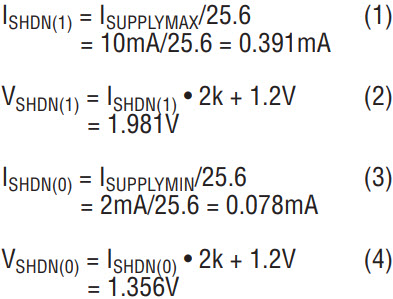
This significant change in the voltage at the SHDN pin is important to consider when determining circuit component values. The Thevenin-equivalent resistance driving the SHDN pin is:

With the control logic low, the following relationship sets the operating current:

where X(0) • VRS/D is the Thevenin voltage contribution from the VRS/D supply:
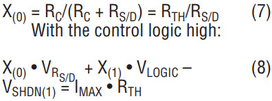
where X(1) • VLOGIC is the additional voltage contribution from the logic input high level:

Considering all the variables and applying some straightforward algebra, a value for the resistor RS/D can be determined from the following equation:

For example, assuming that the RS/D resistor is connected to the driver 12V supply line and that the logic control input comes from a 3.3V logic output, the ideal value for RS/D is 43.7k (43.2k is the nearest 1% tolerance resistor value).
Combining equations 6 and 7, the value for RTH can be found:

Equation 8 can be used to determine the factor X(1); equation 9 then produces the proper value for RC of 8.2k.
Connecting a 43.2k resistor to 12V and an 8.2k resistor to the 0V to 3.3V logic input yields the same result as connecting a single 6.9k resistor to a Thevenin voltage of 4.7V with a logic 1, and 1.8V with a logic 0. These settings will adjust the current of the LT1794 from 10mA per amplifier to 2mA per amplifier.
Four Current Levels from Two Control Inputs
It may also be beneficial to reduce the driver operating current to match the required output power of the driver at any given time. With short loop connections, the full transmitted power is not required, so backing off the driver current to a new minimum level will also help save total system power. What level this current can be needs to be determined from careful characterization with the system transmitting at a specific lower power level.
With two logic control inputs, four operating levels can be obtained. Full power and terminate are the max and min settings, and two other intermediate levels can be set. Figure 5 shows how to implement this extended capability. The values shown will provide operating current levels of 10mA, 7mA, 5mA and 2mA per amplifier in response to the input control bits. This assumes that the RS/D resistor is connected to the driver 12V supply and the input logic level, VC0 and VC1 are 3.3V.
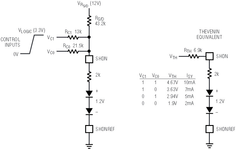
Figure 5. Two logic inputs allow the adjustment of power consumption to data transmission power levels.
The design procedure is the same as with the two level controls, but with two additional states. For the example shown (the logic input levels indicated use VC1 as the MSB and VCO as the LSB, that is binary code 10 is VC1 = 3.3V and VCO = 0V):
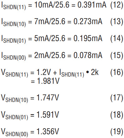
The Thevenin equivalent series resistance is RS/D || RCO || RC1. The four operating states are:
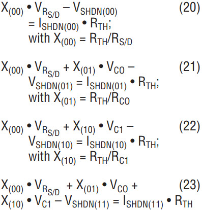
Resistor RS/D can be determined from just the max and min current states:

Then RTH can be found:
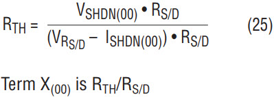
Equation 21 can now be used to determine the factor X(01), then RCO = RTH/X(01). Likewise Equation 22 can determine X(10), then RC1 = RTH/X(10). The design is then complete.
Conclusion
Optimizing power consumption is critical in high port-density central office DSL equipment. The LT1794 is a workhorse power amplifier ideal for driving DSL transmission signals on to the phone line. With built in operating current programmability, the power consumption of the driver can be tailored through the selection of an external resistor. If logic control is available, the power can be adjusted on the fly to match the operating requirements at any given time.
Note: A spreadsheet to perform these calculations is available; contact the author


