PolyPhase Switching Regulators Offer High Efficiency in Low Voltage, High Current Applications
PolyPhase Switching Regulators Offer High Efficiency in Low Voltage, High Current Applications
by
Craig Varga
1998-11-01
Introduction
In recent years, there has been a tendency in the digital world toward smaller device geometries and higher gate counts. This has led to requirements for lower voltages and higher currents for logic supplies. As this trend continues, to levels under 2V and over 30A, the conventional buck regulator approach ceases to be viable. Switch currents are too high for a single device to handle, inductor energy storage exceeds what is available in surface mount technology and ripple current requirements on input capacitors dictate the use of many capacitors in parallel. Although all this may seem like enough of a challenge, the transient response requirements also become much more severe. The question that arises is: “is there a topology that can solve all of these problems simultaneously?” The answer is “PolyPhase™.”
What is PolyPhase, Anyway?
Since it is apparent that multiple FETs need to be paralleled to handle the current requirements, the question is whether there is a way to drive them intelligently, rather than by brute force. The solution is to stagger the turn-on times so that the dead bands in the input current waveform are “filled up,” so to speak. In the simplest implementation, there are essentially two independent synchronous buck regulators operating 180° out of phase. The net effect of this is that the input and output ripple currents of the two channels tend to cancel during steady-state operation. This results in significant reductions in both input and output capacitor requirements. There is also a fourfold reduction in the total inductor energy storage requirement, which means much smaller inductors and vastly improved transient dynamics. During a large load step, the two channels operate at maximum duty factor in an attempt to maintain the desired output voltage. Both inductor currents slew rapidly and are now additive, since they are going in the same direction. Hence, the slew rate is double what a single channel could do for equal inductor values. However, due to the ripple current cancellation during steady-state conditions, the two inductors can be reduced to approximately one-half the value that a single channel design would require for equal ripple currents. Since during slew they appear to be operating in parallel, the actual slew rate is four times that of a single channel design with equal steady-state output ripple current. Both input and output ripple frequencies are double those of a single-channel design, further simplifying filtering requirements.
Why Stop at Two?
If two channels are good, aren’t more channels better? In a word, yes. In principle, there is no limit to the number of parallel channels that can be added. As the number of channels, n, increases, the ripple frequency increases to n times the single-channel frequency. Input and output RMS ripple currents continue to decrease. Diminishing returns are reached as n rises above three. At three stages, the ripple reductions are very substantial and dynamic performance is excellent. Adding more channels produces slight improvements but the dramatic gains will have been realized by n = 3. The only real penalty is added complexity.
Another aspect worth considering is expandability. It is reasonable with today’s technology to build a single stage, all surface mount, synchronous buck regulator capable of approximately 15 amps continuous output current. At higher current levels, power dissipation in individual devices becomes difficult to manage. Gate drive capability of driver ICs is somewhat limited and is incapable of driving enough paralleled MOSFETs to handle larger currents at high frequencies. Inductors capable of greater energy storage cannot be obtained in surface mount technology. Therefore, if currents substantially greater than 15 amps are required, it is a simple matter of paralleling additional stages to obtain the higher currents. For 30 amps, use two stages. At 45 amps, use three stages and so on. As more stages are added, the ripple currents are further reduced, so there is no need to add large quantities of input or output capacitors to handle the higher current capability.
The bottom line is that PolyPhase designs offer a considerable reduction in the cost and volume of the power devices at the expense of a little added complexity in the control circuitry.
2-Phase Design Example
The circuit shown in Figure 1 is a 2-phase, voltage mode–control, synchronous buck regulator designed for a 5V input and output voltages below 3.3V. It is intended to power large memory arrays, ASICs, FPGAs and the like in server and workstation applications. The output is capable of more than 30 amps continuous at outputs of 2.5V and below, with peak current capability of greater than 40 amps. The design is entirely surface mount and the maximum height above the board is 5.5mm. Overall board area is only 4.24 in2. Efficiency is excellent, as can be seen in the curve in Figure 2. Output ripple voltage is shown in Figure 3. The circuit’s dynamic response to a 10 amp load step is shown in Figure 4. The response is dominated by the output capacitor’s ESR and shows the output voltage recovered to the original level in under 10µs. Figures 5 and 6 show how the input and output ripple currents cancel.

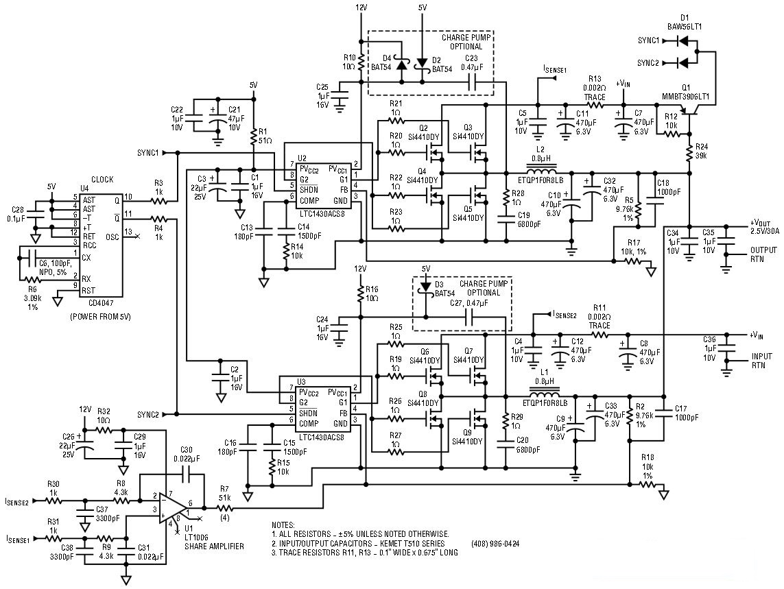
Figure 1. 2-phase synchronous buck regulator.

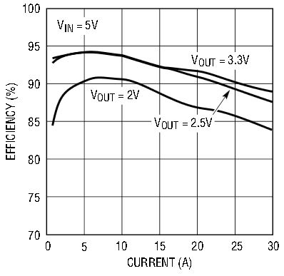
Figure 2. Efficiency of Figure 1’s circuit, VIN = 5V.

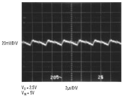
Figure 3. Output ripple with 30A load.

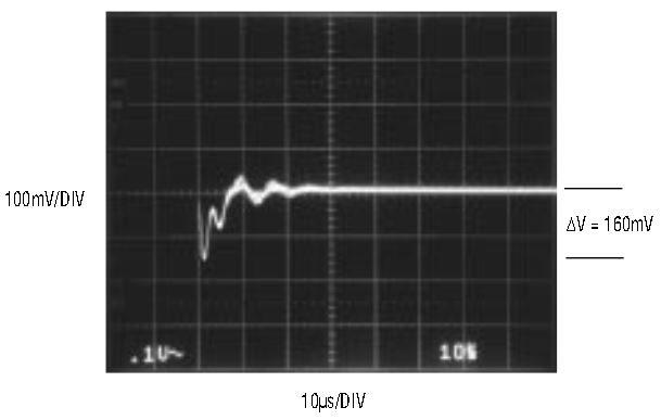
Figure 4. Transient response with 10A load step (100ns rise time).

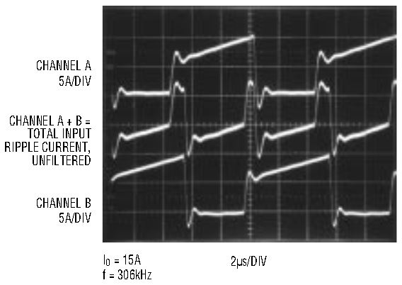
Figure 5. Ripple cancellation—input.

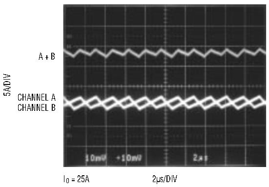
Figure 6. Ripple cancellation—output.
Circuit Operation
The basic design consists of two LTC1430CS8-based synchronous buck regulators connected in parallel and operated 180° out of phase. U4, the CD4047 oscillator, is used to generate the required clock signals and synchronize the two LTC1430s. Unfortunately, simply connecting two regulators in parallel is a recipe for instant disaster. The output voltages of the two regulators will be slightly different due to normal component tolerances. Therefore, the higher output voltage channel will attempt to supply the full load current, while the lower voltage output will sink current from the output in a desperate attempt to reduce the output voltage to where it thinks it should be. The result is like a dog chasing its tail, with large currents running around in a circle and going nowhere.
Op amp U1 solves this problem. Because the two channels are identical, if the output currents are the same, the input currents will be also. Low value sense resistors are included in the input power path to allow the circuit to measure input current. U1 then forces the input current of channel two to match the input current of channel one by making small adjustments in channel two’s output voltage. It does this by adding or subtracting a small amount of current from channel two’s feedback divider. The two sense resistors are short lengths of PCB trace and only need to be ratiometrically accurate. Absolute value of these resistors is not important (see Linear Technology Application Note 69, Appendix A, for a discussion on how to design trace resistors).
The only remaining trick in the circuit is the role of Q1 and its associated circuitry. At start-up, the LTC1430’s clock frequency is slowed down to approximately 10kHz until the output voltage rises to approximately 50% of the desired level. If, during this start-up phase, an attempt is made to synchronize the controller to a very high frequency, the oscillator ramp amplitude never rises to a level sufficiently high to trip the PWM comparator and enable the FET drivers. Therefore, the output gets stuck on ground. Q1 fixes this by forcing the sync signals high during the turn-on transient. Once the output voltage nears its final level, the clock signals are allowed to synchronize the two PWM controllers.
Conclusion
The design shown combines the performance characteristics that will be required to power the digital systems that will emerge over the next several years. Circuits based on these concepts will be able to efficiently deliver very high current at low voltage while relying on surface mount technology to maintain low profile and minimum use of real estate. They will also provide substantially better dynamic performance than has been available using more conventional design methodologies and do all of this at a reasonable cost.
关于作者
关联至此文章
产品


