Micropower SOT-23 Buck Regulator Accepts Inputs to 34V
Introduction
The LT1934 is a micropower buck regulator with an internal 400mA power switch. It provides up to 300mA output current, while consuming just 12µA of quiescent current, an important feature for always-on battery-powered applications such as laptop computer standby supplies or remote instrumentation that must operate for years from primary batteries. Its wide input voltage range of 3.4V to 34V makes it applicable to a variety of power sources including 24V industrial supplies, automotive batteries and unregulated wall transformers.
3.3V 250mA Supply from 24V Input Consumes Just 15µA
Figure 1 shows a 3.3V/250mA supply that accepts inputs from 4.5V to 34V. With the output in regulation and with no load, the input current with VIN = 24V is less than 15µA. Input current falls to less than 1µA when the LT1934 is placed in shutdown mode by pulling SHDN to ground. The SHDN pin can be tied to VIN if the shutdown mode is not used. The capacitor and diode tied to the BOOST pin provide a bias voltage above VIN in order to fully saturate the internal NPN power switch, thereby maintaining high efficiency over the entire input voltage range.


Figure 1a. This buck regulator supplies 250mA at 3.3V from an input voltage as high as 34V. Input current with no load applied is less than 15µA.

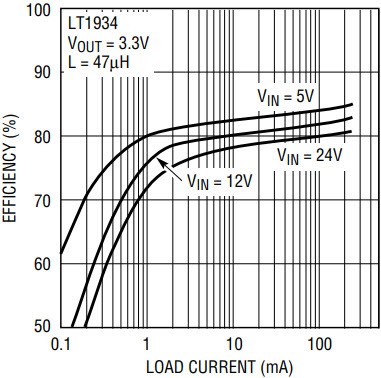
Figure 1b. Efficiency of Figure 1’s circuit.
The LT1934 uses Burst Mode® operation, with low quiescent current, to achieve high efficiency across a wide range of load currents, as shown in Figure 1b. An internal comparator monitors the voltage at the FB pin. When the voltage at this pin is above 1.25V, the LT1934 is in its sleep mode with only its reference and feedback comparator biased. In this state the VIN pin current is 12µA. As the load current discharges the output capacitor, the FB pin voltage falls below 1.25V and the comparator enables the internal oscillator and drive circuits. The LT1934 switches with a fixed off time of 1.8µs, limiting the peak inductor current to 400mA as it delivers power to the output. Figure 2 shows the operating waveforms of the circuit in Figure 1a. Output voltage ripple is less than 50mVP–P. Figure 3a shows a circuit that generates 5V from a 6.5V–34V input. Figure 3b shows the efficiency of this circuit.

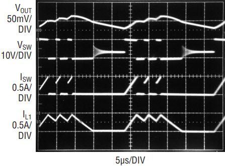
Figure 2. The operating waveforms of the circuit in Figure 1 as it delivers 180mA from a 10V input. The fast, accurate, cycle-by-cycle current limit results in a robust circuit that can withstand a shorted output.

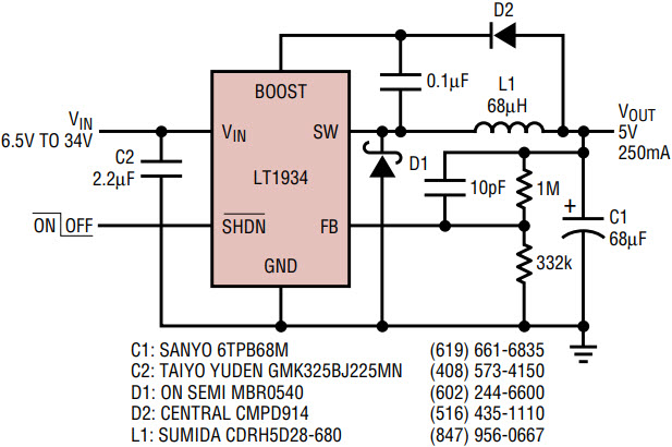
Figure 3a. The LT1934 provides 250mA at 5V.

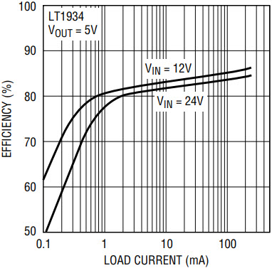
Figure 3b. Efficiency of Figure 3’s circuit.
The accurate, fast, cycle-by-cycle current limit of the LT1934 keeps the switch and inductor currents under control at all times. In addition, the 1.8µs switch off time is extended during fault conditions when the output voltage is pulled below the programmed output voltage. This ensures that the LT1934 can handle a shorted output.
The LT1934-1 for Low Current Supplies
The LT1934-1 is identical to the LT1934 except that the current limit is 120mA. The LT1934-1 can be used in applications with a maximum load current of 60mA. This lower current limit allows a better match between the power components (the inductor and the input and output capacitors) and the application, resulting in a smaller circuit size. Input ripple is also lower, reducing noise and simplifying input filtering. The LT1934-1 may be a better choice when the power source has a high output impedance, such as 4mA-20mA loops, long-life primary batteries with high internal resistance or remote supplies with long cables. Low maximum switch current is also helpful in designing intrinsically safe systems, which have limits on stored energy and require current limiting resistors in series with external connections. Figure 4 shows a 3.3V supply implemented with the LT1934-1.

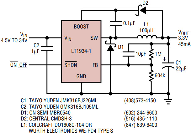
Figure 4. Smaller components can be used with the lower current LT1934-1.
Li-Ion Battery Charger with Industrial Input Range
The circuit in Figure 5 is a complete, single-cell Li-Ion battery charger that operates from an input of 7V to 28V and provides a charge current of 350mA. This charger requires no microcontroller. A charge cycle is initiated when power is applied to the circuit, and end-of-charge is indicated when the battery voltage reaches 4.2V and charge current has fallen to one tenth of the nominal charge current.

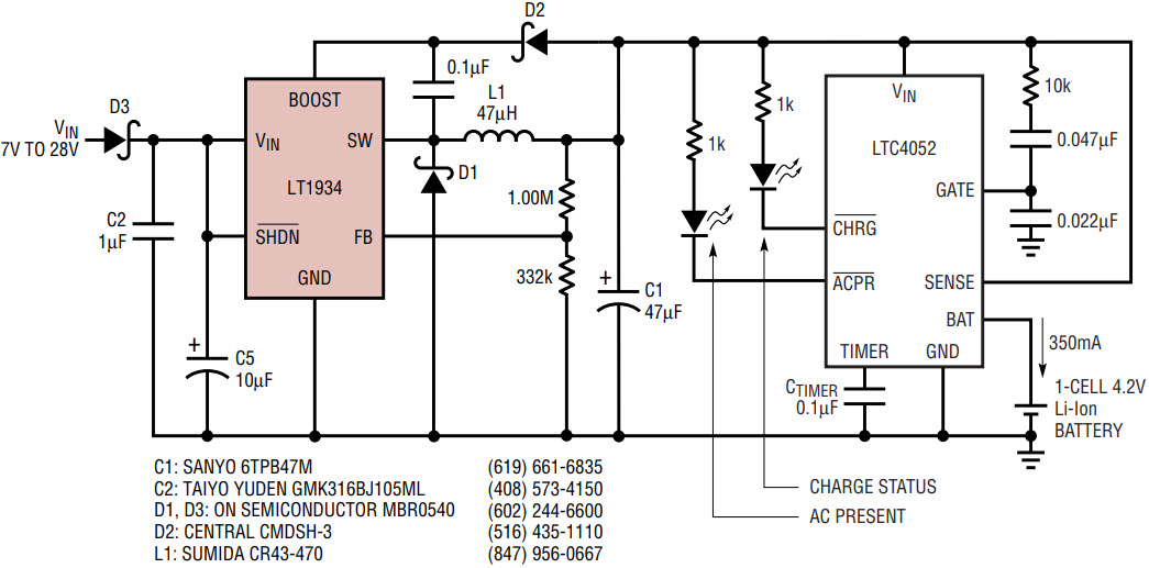
Figure 5. This standalone 350mA Li-Ion battery charger accepts inputs to 28V and requires no heat sinks.
The LT1934 acts as a current-limited 5V pre-regulator for the LTC4052-4.2 pulse charger. The LTC4052 monitors the battery voltage and pulls the CHRG pin low to indicate that the battery is being charged.
If this voltage is less than 2.5V, the LTC4052 applies a 24mA trickle charge, with the LT1934 maintaining 5V across C1.
When the battery voltage rises above 2.5V, the LTC4052 enters its fast charge mode, turning on an internal N-channel FET switch between its SENSE and BAT pins. This connects the LT1934’s output to the battery. As the voltage across C1 falls to the battery voltage, the LT1934 limits its output current, charging the battery at 350mA. Because the FET is fully on, very little power is dissipated, and the charging circuit maintains high efficiency during the entire charge cycle.
When the battery voltage reaches 4.2V, the LTC4052 turns off the switch for 100ms. If the battery voltage falls below 4.2V during this period, the switch is turned back on for at least 400ms. In this manner, the LTC4052 modulates the duty cycle of the 350mA current source. When this duty cycle falls to 10%, the LTC4052 indicates that the battery is nearly charged by switching the CHRG pin to a weak 40µA pull down. Pulse charging continues until a timer in the LTC4052 stops the charge cycle after three hours, when the CHRG pin goes to a high impedance state. If the battery voltage is pulled below 4.05V due to a load current, the LTC4052 reenters its fast charge mode.
If input power is removed, the LTC4052 isolates the LT1934’s circuitry and reduces battery load to less than 1µA. Diode D3 provides reverse input protection.
The LT1934 regulates its output current by limiting the peak current in L1 to 400mA. The charge current equals the average current in L1, and depends on the input and output voltages, as shown in Figure 6. In addition to these variations, expect approximately ±15% variation in the nominal charge current due to variations in the current limit and switch off time of the LT1934 and the value of L1.

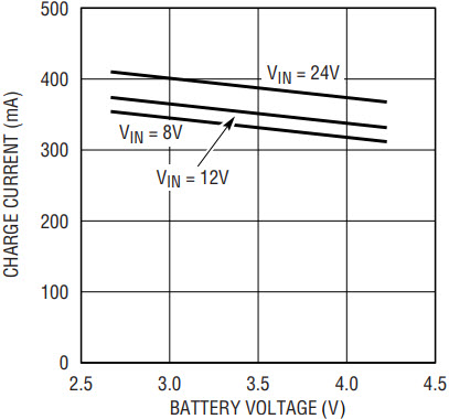
Figure 6. Charging current as a function of battery voltage and input voltage.
In addition to indicating charge status, the LTC4052 also provides an AC-present flag that indicates that power has been applied to the charger. A similar device, the LTC1730, can be used to provide additional features, including a thermistor interface for monitoring the temperature of the battery and a shutdown pin that can be used to reinitialize the charge cycle timer.
This Li-Ion charger uses only surface mount devices, requires no heat sinks, and its wide input voltage range accepts a variety of power sources including unregulated wall transformers, car batteries and 24V industrial supplies. The charger is completely standalone, requiring no microcontroller coding. On the other hand, its charge status and AC-present pins provide useful information to the user through LEDs or to a microcontroller through a few digital I/O pins, making it simple to integrate into a battery powered system.
Hot Plugging Safely
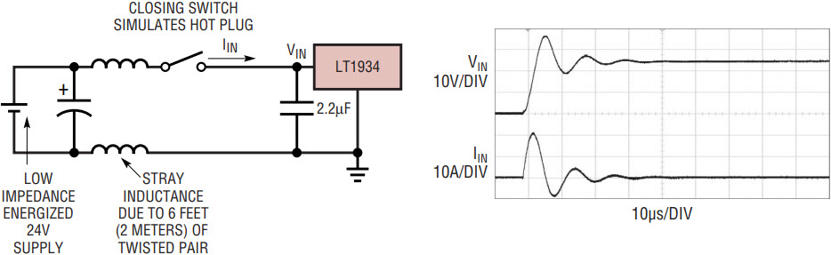
The small size, robustness and low impedance of ceramic capacitors make them an attractive option for the input bypass capacitor of LT1934 and LT1934-1 circuits. However, these capacitors can cause problems if the LT1934 is plugged into a live supply.1 The low-loss ceramic capacitor combined with stray inductance in series with the power source forms an underdamped tank circuit, and the voltage at the VIN pin of the LT1934 can ring to twice the nominal input voltage, possibly exceeding the LT1934’s rating and damaging the part. If the input supply is poorly controlled or the user will be plugging the LT1934 into an energized supply, the input network should be designed to prevent this overshoot.
Figure 7 shows the waveforms that result when an LT1934 circuit is connected to a 24V supply through six feet of 24-gauge twisted pair. The first plot is the response with a 2.2µF ceramic capacitor at the input. The input voltage rings as high as 35V, and the input current peaks at 20A. One method of damping the tank circuit is to add another capacitor with a series resistor to the circuit. In Figure 7b an aluminum electrolytic capacitor has been added. This capacitor’s high equivalent series resistance damps the circuit and eliminates the voltage overshoot. The extra capacitor improves low frequency ripple filtering and can slightly improve the efficiency of the circuit, though it is likely to be the largest component in the circuit. An alternative solution is shown in Figure 7c. A 1Ω resistor is added in series with the input to eliminate the voltage overshoot (it also reduces the peak input current). A 0.1µF capacitor improves high frequency filtering. This solution is smaller and less expensive than the electrolytic capacitor. For high input voltages its impact on efficiency is minor, reducing efficiency less than one half percent for a 5V output at full load operating from 24V.

a.

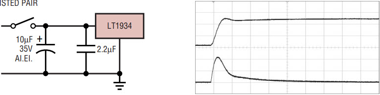
b.

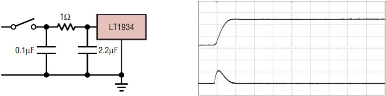
c.

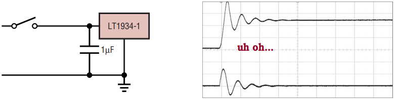
d.

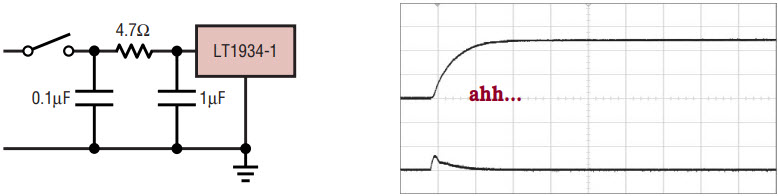
e.
Figure 7. A well chosen input network prevents input voltage overshoot and ensures reliable operation when the LT1934 is connected to a live supply.
Voltage overshoot gets worse with reduced input capacitance. Figure 7d shows the hot plug response with a 1µF ceramic input capacitor, with the input ringing above 40V. The LT1934-1 can tolerate a larger input resistance, such as shown in Figure 7e where a 4.7Ω resistor damps the voltage transient and greatly reduces the input current glitch on the 24V supply.
Conclusion
The LT1934’s 34V input range and short circuit robustness make it a great choice for small industrial systems. It delivers up to 300mA output with an all-surface-mount circuit that requires no heat sinks. The integrated power switch, SOT-23 package and high frequency operation result in a very small regulator, requiring less than one square centimeter of PCB area. Efficiency is high over the entire load range, with the 12µA quiescent current extending battery life.
Notes
1. See Linear Technology Application Note 88 for a complete discussion.
关于作者


