Maximize Apollo MxFE™ Spectrum Equalization Performance—Part 1: PFILT and CFIR Fundamentals

Maximize Apollo MxFE™ Spectrum Equalization Performance—Part 1: PFILT and CFIR Fundamentals
2026-11-10
Key Takeaways
|
Abstract
As an IC incorporating state-of-the-art data converters, the Apollo MxFE family is engineered with highly programmable digital signal processing (DSP) capabilities to complement the data conversion process. Among these capabilities, the programmable finite impulse response (FIR) filter (PFILT) and complex FIR filter (CFIR) can be leveraged to implement a variety of signal conditioning algorithms, including spectrum equalization. To achieve power efficiency, the PFILT and CFIR are designed with a limited number of taps, which introduces potential constraints on performance. This article explores unique approaches to maximize spectrum equalization performance by leveraging the flexibility of the Apollo MxFE DSP architecture. Part 1 of this article focuses on the fundamental principles, operating modes, and architectural flexibility of the Apollo MxFE PFILT and CFIR blocks. These concepts establish the foundation for creative spectrum equalization techniques presented in Part 2.
Apollo MxFE Data Path Overview
The Apollo MxFE family is made up of software-defined, high-performance, wideband direct-sampling mixed-signal front end (MxFE) technology, including the AD9084 and AD9088. At its core, Apollo MxFE technology integrates multiple high-speed data converters—four in the AD9084 and eight in the AD9088. It supports RF bandwidth up to 18GHz, enabling coverage across L-, S-, C-, X-, and Ku-bands.
Beyond its data converters, Apollo MxFE technology distinguishes itself through a rich and highly flexible digital signal processing (DSP) architecture. Built-in capabilities such as the spectrum sniffer, programmable finite impulse response (FIR) filter (PFILT), complex FIR (CFIR), coarse and fine digital downconverters (CDDC/FDDC) and upconverters (CDUC/FDUC), and the fractional sample rate converter (FSRC) allow both transmit (Tx) and receive (Rx) signals to be conditioned directly on chip. By moving signal conditioning closer to the data converters, Apollo MxFE technology reduces sample rate requirements and power consumption of adjacent digital devices. This makes it particularly well suited for demanding applications such as phased array radar, communications, and instrumentation.
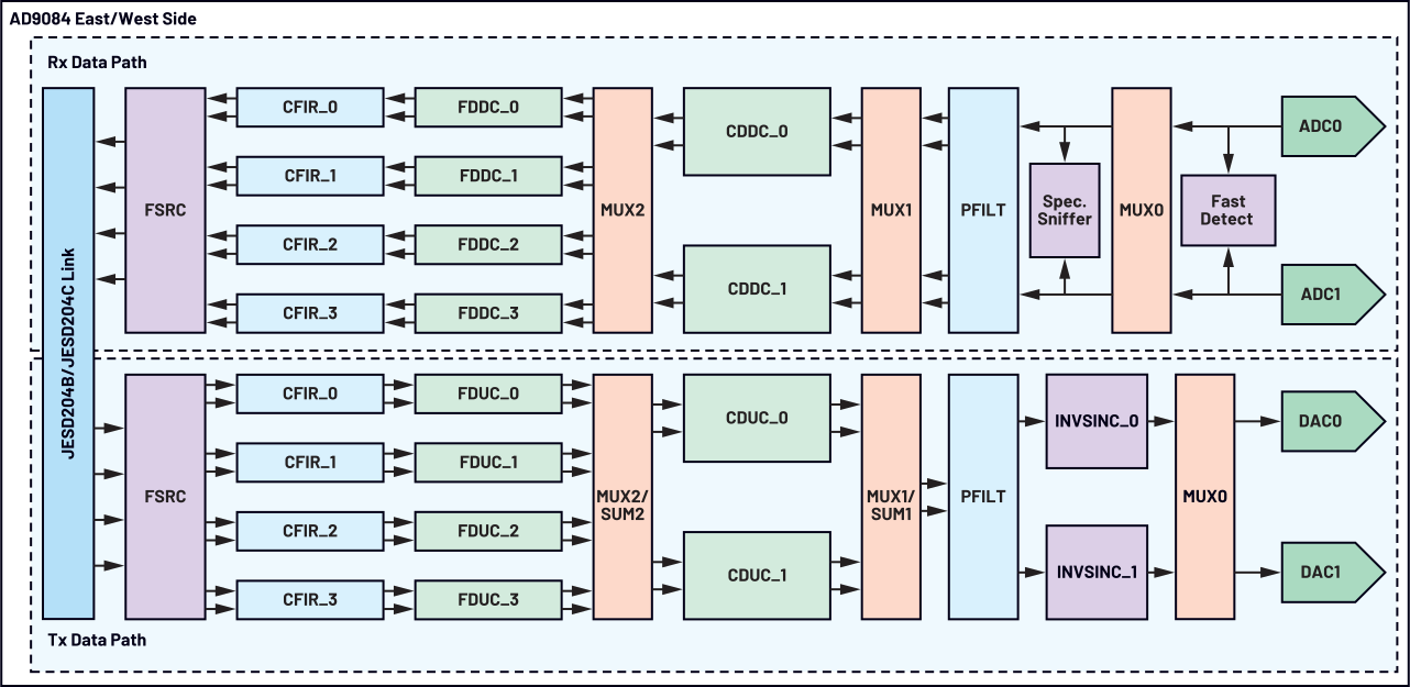
Figure 1 illustrates a high-level view of the AD9084 data path. The device is architecturally symmetric, with independent east and west sides, each containing a complete receive and transmit data path. For clarity, only one side and the primary DSP blocks are shown. The AD9088 follows a similar structure but doubles the number of converter cores and omits certain DSP features, such as the FSRC.
Receive Data Path
In the receive data path, pairs of ADC outputs—either I/Q or dual real signals—are first processed by the fast detect block to support gain control. These signals are then routed through flexible multiplexing (MUX0) to feed both the spectrum sniffer and PFILT.
The spectrum sniffer provides rapid detection of spectral activity within the digitized bandwidth, enabling fast signal awareness. The PFILT performs front-end signal conditioning, supporting functions such as spectrum equalization and quadrature error correction (QEC). Operating at the full ADC sample rate, the PFILT supports up to 32 FIR taps and produces two pairs of output signals.
These outputs are routed via MUX1 into two CDDC blocks, each combining optional digital downconversion with configurable decimation filtering. Further downstream, MUX2 distributes the resulting signals to as many as four FDDC blocks, enabling additional frequency translation and decimation. This multistage structure allows efficient extraction of multiple sub-bands—an essential capability for multiband systems.
Following each FDDC, a CFIR block provides additional filtering at a reduced sample rate. The CFIR plays a key role in compensating residual magnitude and phase distortions not addressed by the PFILT in earlier analog/digital stages. It supports two modes: normal mode with up to 16 taps, and sparse mode with up to 128 taps (with up to 16 non-zero taps).
At the end of the receive chain, the FSRC provides optional fractional decimation to match the desired output rate before data is transmitted off-chip via the JESD204B/JESD204C interface.
Transmit Data Path
The transmit data path mirrors the receive chain in reverse. Incoming data from the JESD interface may first pass through the FSRC for fractional rate conversion. Up to four CFIR blocks can then be applied for pre-equalization, compensating for spectrum distortions introduced by downstream digital/analog components.
Subsequently, the FDUC and CDUC blocks perform frequency translation and interpolation using programmable interpolation factors. MUX2 is used to multiplex the FDUC outputs to produce input signals for CDUC. In addition, transmit MUX2 provides additional flexibility by allowing outputs from multiple FDUCs to be combined before feeding into the CDUCs.
Further downstream, MUX1 routes the output signal from CDUC into the PFILT, which performs additional conditioning before passing outputs to the inverse sinc (INVSINC) blocks. Similar to MUX2, MUX1 can optionally sum the two CDUC outputs. Unlike the receive data path, the PFILT in the transmit data path generates only one pair of output signals, in which each component is further used by the following INVSINC blocks to pre-compensate the DAC sinc (sin(x)/x) roll-off. Finally, the processed digital signals are converted into analog by the DACs.
Flexibility and Configuration Challenge
A defining feature of Apollo MxFE technology is its architectural flexibility. Nearly every DSP block can be independently enabled, bypassed, or reconfigured for different operation modes, and multiple routing paths can be constructed using programmable multiplexers. This allows the data path to be tailored for a wide range of sample rates, signal formats (real or complex), and performance targets.
However, this flexibility comes at a cost: identifying the optimal configuration is nontrivial. This article addresses that challenge by exploring creative approaches for maximizing spectrum equalization performance using PFILT and CFIR, leveraging the full capability of Apollo MxFE programmable DSP architecture.
Apollo MxFE PFILT and CFIR Architectures
As discussed earlier, the PFILT and CFIR blocks are user-programmable and can be configured to implement a variety of signal-conditioning algorithms. An important application of PFILT and CFIR is spectrum equalization, which plays a critical role in wideband RF transceiver performance.
Spectrum distortion degrades system performance by increasing error vector magnitude (EVM) and reducing demodulation accuracy. Spectrum equalization mitigates these distortions, enabling operation within the optimal dynamic range and, in many cases, improving overall signal-to-noise ratio (SNR).
PFILT Operation Modes
Each Apollo MxFE PFILT contains a total of 32 real FIR taps. Depending on the selected operating mode, these taps are partitioned among multiple sub-filters, as summarized in Table 1.
| PFILT Mode | Explanation | Main Application |
|
16-Tap Dual Real Mode |
One PFILT contains two independent 16-tap real sub-filters, one for each ADC or DAC channel (see Figure 2). |
Spectrum equalization |
|
32-Tap Single Real Mode |
One PFILT contains a single 32-tap real filter assigned to a single ADC or DAC channel (see Figure 2). |
Spectrum equalization |
|
8-Tap Dual Real Mode |
One PFILT contains two independent 8-tap real sub-filters, one for each ADC or DAC channel (see Figure 2). |
Spectrum equalization |
|
Half-Complex Mode |
One PFILT contains two 16-tap sub-filters: a direct-term filter and a cross-term filter. The direct-term filter processes an input signal and returns the filtered result to the same path. The cross-term filter processes one input signal and couples the filtered result into the other signal path (see Figure 3). |
QEC |
|
Matrix Mode |
One PFILT contains four 8-tap sub-filters. Each input signal is processed by both a direct FIR filter and a cross-term FIR filter. This configuration allows linear RF equalization and QEC to be performed simultaneously when sufficient filter taps are available (see Figure 3). |
Simultaneous QEC and spectrum equalization |
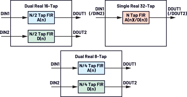
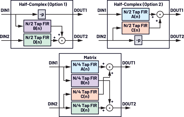
As shown in Figure 2 and Figure 3, each PFILT accepts two input signals, DIN1 and DIN2. Depending on the configuration, DIN1 and DIN2 may represent either two independent real signals or the I and Q components of a complex signal. After filtering, the PFILT generates two output signals, DOUT1 and DOUT2.
PFILT Data Path Connectivity
Figure 4 and Figure 5 illustrate the connectivity between the PFILT and adjacent processing blocks in the receive and transmit data paths, respectively.
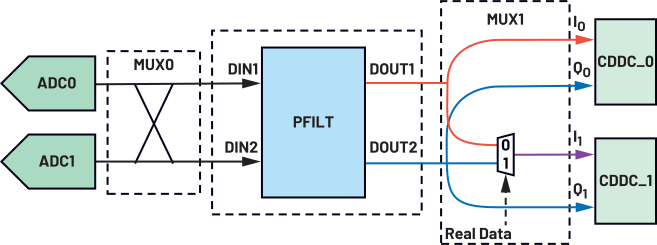
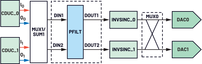
In the receive data path as shown in Figure 4, MUX0 can be configured to route ADC outputs to DIN1 and DIN2 using any of the combinations listed in Table 2.
|
Rx MUX0 Combination Mode |
Description |
| 1 | DIN1 = ADC0, DIN2 = ADC1 |
| 2 | DIN1 = ADC1, DIN2 = ADC0 |
| 3 | DIN1 = ADC0, DIN2 = ADC0 |
| 4 | DIN1 = ADC1, DIN2 = ADC1 |
MUX1 combines DOUT1 and DOUT2 to generate two pairs of complex signals, one pair for each CDDC.
For CDDC_0:
- I0 = DOUT1
- Q0 = DOUT2
For CDDC_1:
- Q1 = DOUT2
- I1 = either DOUT1 or DOUT2
When the PFILT inputs are real-valued signals, I1 = DOUT2. Otherwise, I1 = DOUT1.
In the transmit data path as shown in Figure 5, MUX1/SUM1 combines two pairs of complex signals from CDUC_0 and CDUC_1 to generate PFILT inputs DIN1 and DIN2.
Four operating modes are supported, as summarized in Table 3.
|
Tx MUX1/SUM1 Combination Mode |
Description |
| 1 | DIN1 = I0, DIN2 = I1 |
| 2 | DIN1 = I0 + I1, DIN2 = Q0 + Q1 |
| 3 | DIN1 = I0, DIN2 = Q0 |
| 4 | DIN1 = I1, DIN2 = Q1 |
After filtering, DOUT1 is routed to INVSINC_0, and DOUT2 is routed to INVSINC_1. The transmit path MUX0 operates similarly to the receive path MUX0, generating the input signals for DAC0 and DAC1.
CFIR Operation Modes
The Apollo MxFE CFIR supports two operating modes: normal mode and sparse mode. In normal mode, the CFIR functions as a conventional FIR filter with up to 16 complex-valued taps. In sparse mode, the effective filter length can be extended to as many as 128 complex taps while restricting the number of non-zero taps to 16. This capability is particularly useful when compensating systems with long-delay responses, such as cable reflections, antenna mismatches, analog front-end echoes, or other multipath effects.
As shown in Figure 1, each receive or transmit data path in the AD9084 can contain up to four CFIR blocks (eight CFIR blocks in the AD9088). Table 4 summarizes the maximum number of CFIR blocks under different FDUC/FDDC operation conditions. When the FDUC or FDDC interpolation/decimation factor is greater than 1, each CFIR can process twice as many data streams. This allows a single RF carrier (one FDUC/FDDC) to be split into two independent RF carriers, each with its own CFIR filter response.
|
FDUC/FDDC Mode |
Maximum Number of CFIRs for Each Data Path | Maximum I/Q Sample Rate of Each CFIR | |
|
AD9084 |
Interpolation/decimation factor >1 |
Four CFIRs |
2.5GSPS |
| Interpolation/decimation factor = 1 |
Two CFIRs |
5GSPS |
|
|
AD9088 |
Interpolation/decimation factor >1 |
Eight CFIRs |
1.25GSPS |
| Interpolation/decimation factor = 1 |
Four CFIRs |
2.5GSPS |
Normal CFIR Mode
Normal mode can be expressed by the following equation:

where:
- x(n) is the CFIR input signal,
- CFIR16 (k) (k = 0,1,…15) denotes the CFIR coefficients, and
- y(n) is the CFIR output signal.
The input samples, filter coefficients, and output samples may all be complex-valued.
Sparse CFIR Mode
In sparse mode, the 16-tap CFIR architecture can be extended to span an impulse response of up to 128 samples while maintaining a maximum of 16 non-zero coefficients.
Figure 6 illustrates how the 16 active taps are selected from a delay line containing 128 samples. The delay line is organized into eight data stores (Dstore0 to Dstore7), each containing 16 complex (I/Q) samples.
The four lower data stores (Dstore0, Dstore2, Dstore5, and Dstore7) provide inputs directly to the Dpath_mux block. The remaining data stores (Dstore1, Dstore3, Dstore4, and Dstore6) are used to introduce additional delay between adjacent lower data stores.
The Dpath_mux receives a total of 64 candidate samples from Dstore0, Dstore2, Dstore5, and Dstore7 and selects 16 of them according to the configuration of hsel.
Dstore2
The contents of Dstore2 depend on mem_sel0:
- mem_sel0 = 0: Dstore2 contains the next contiguous 16 samples following Dstore0:
x[n – 16], x[n – 17],…, x[n – 31]
- mem_sel0 = 1: Dstore2 contains samples delayed by an additional 16 samples through Dstore1:
x[n – 32], x[n – 33],…,x[n – 47]
Dstore5
The contents of Dstore5 are determined by mem_sel1:
- mem_sel1 = 0: No additional delay is inserted.
- mem_sel1 = 1: An additional 16-sample delay is inserted through Dstore3.
- mem_sel1 = 2: An additional 32-sample delay is inserted through Dstore3 and Dstore4.
Dstore7
The contents of Dstore7 are controlled by mem_sel2:
- mem_sel2 = 0: No additional delay is inserted.
- mem_sel2 = 1: An additional 16-sample delay is inserted through Dstore6.
hsel Tap Selection
The hsel parameter specifies the locations of up to 16 non-zero taps. Each hsel value ranges from 0 to 63 and selects one sample from the 64 candidate inputs provided by Dstore0, Dstore2, Dstore5, and Dstore7.
The mapping is:
- Values 0 to 15 select samples from Dstore0.
- Values 16 to 31 select samples from Dstore2.
- Values 32 to 47 select samples from Dstore5.
- Values 48 to 63 select samples from Dstore7.
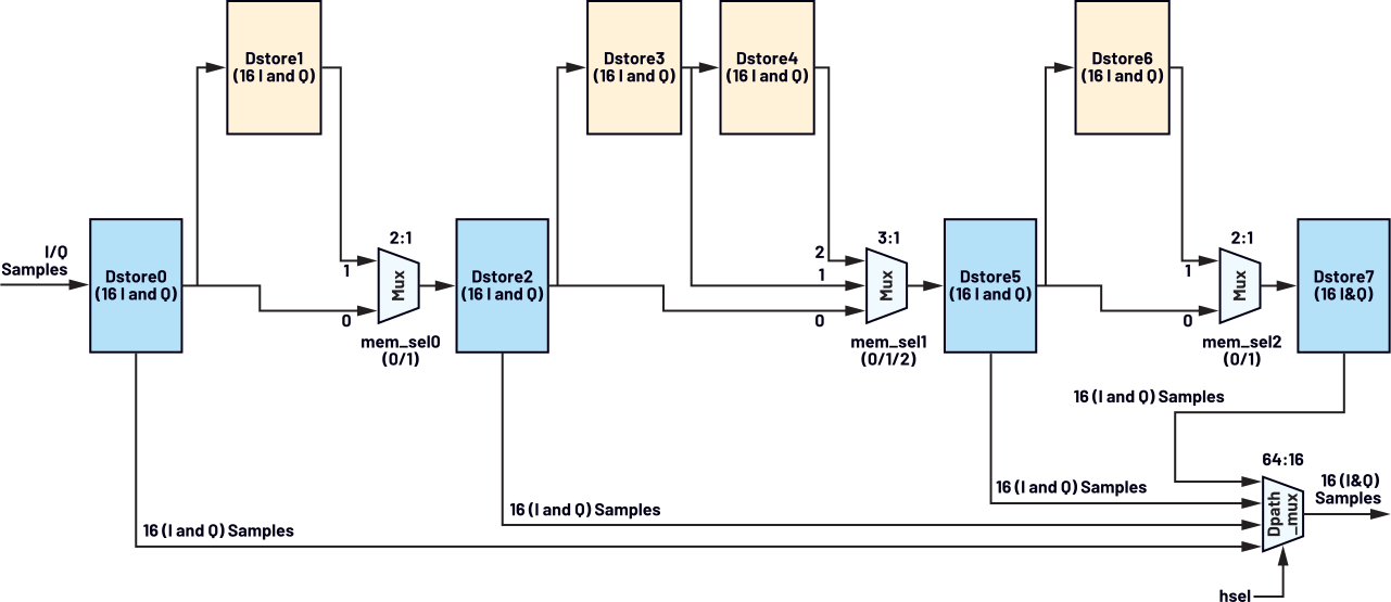
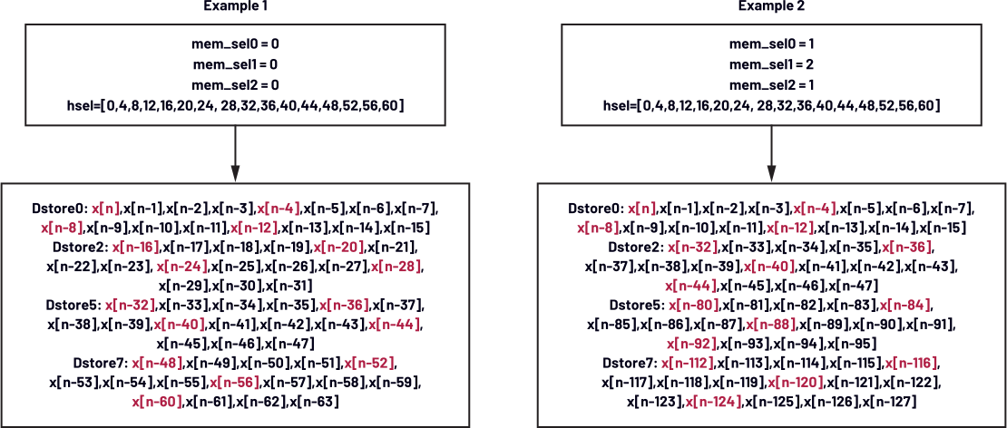
Figure 7 illustrates two examples showing how the locations of the 16 active taps can be configured using different combinations of mem_sel[2:0] and hsel.
Sparse Mode Constraints
As shown in Example 2 in Figure 7, the sample ranges represented by Dstore0, Dstore2, Dstore5, and Dstore7 may not be contiguous. This imposes restrictions on the allowable hsel selections.
The CFIR produces two consecutive output samples during each clock cycle. Consequently, whenever sample x[k] is selected, the previous sample x[k – 1] must also be available. For discontinuous Dstore configurations, x[k – 1] may not exist within the accessible sample set, preventing x[k] from being selected.
As a result:
- In Example 2, hsel values 15, 31, 47, and 63 cannot be selected.
- In Example 1, although the four Dstores form a contiguous sample range, the final sample corresponding to hsel = 63 still cannot be selected.
Subject to these constraints, the 16 non-zero taps may be placed at arbitrary locations within the 128-sample impulse response window.
MUX2 Data Path Connectivity
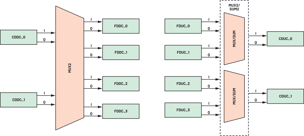
MUX2 routes signals between the FDDC/FDUC and CDDC/CDUC blocks in both the receive and transmit data paths, as shown in Figure 8.
In the receive data path, each FDDC can select its input from either CDDC_0 or CDDC_1.
In the transmit data path:
- CDUC_0 can select the output of FDUC_0, FDUC_1, or the sum of FDUC_0 and FDUC_1.
- CDUC_1 can select the output of FDUC_2, FDUC_3, or the sum of FDUC_2 and FDUC_3.
Conclusion
Part 1 of this article series introduced the fundamentals of Apollo MxFE PFILT and CFIR operation and explored the flexibility of the Apollo MxFE DSP architecture, providing the foundation for understanding the resources available for spectrum equalization. Part 2 builds upon these fundamentals and presents creative approaches for maximizing spectrum equalization performance within the limited PFILT and CFIR tap resources. It demonstrates how the flexibility of the Apollo MxFE DSP architecture can be leveraged to address challenging equalization requirements and achieve improved system performance.
关于作者
Mizhou (Michelle) Tan是ADI公司的产品应用工程师。3年来,她一直为RF收发器产品和应用的设计和开发提供支持。在加入ADI公司之前,她获得了四川大学电气工程学士学位和硕士学位,并于2004年获得了新泽西理工学院电气和计算机工程博士学位。从2004年至2018年,她分别在Agere Systems、LSI Logic和Intel Corp.担任算法、系统和软件工程师。她在技术会议和期刊上发表论文15余篇