LTC2050, Zero-Drift Operational Amplifier in SOT-23 Package Minimizes Board Area without Compromising Specs
LTC2050, Zero-Drift Operational Amplifier in SOT-23 Package Minimizes Board Area without Compromising Specs
2000-02-01
Introduction
The LTC2050 is a zero-drift operational amplifier available in the 5- or 6-lead SOT-23 and SO-8 packages. It minimizes board area while providing uncompromising DC performance, including 3µV (max) DC offset and 30nV/°C (max) DC offset drift. It operates from a 2.7V supply while still supporting 5V applications. The power consumption is 800µA and the versions in the 6-lead SOT-23 and SO-8 packages offer power shutdown.
Other key features of this new device include:
- Small 5- or 6-lead SOT-23 package
- 2.7V operation
- 3µV maximum offset voltage
- 30nV/°C maximum offset voltage drift
- 1.5µVP-P typical noise (0.1Hz to 10Hz)
- More than 130dB of DC PSRR, CMRR and gain (typical)
- Output swings rail-to-rail with 1kΩ loads
- Extended common mode input range
- Power shutdown below 10µA (available in 6-lead SOT-23 and SO-8)
Extended Input Common Mode Range with Uncompromising CMRR
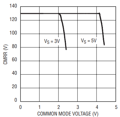
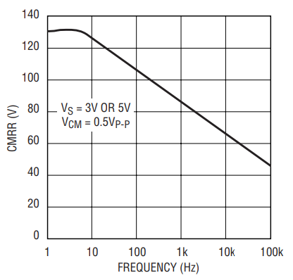
At room temperature, with the input common mode level at mid-supplies, the LTC2050 typically has 0.5µV of input-referred offset (input-referred offset is guaranteed to be less than ±3µV). To ensure this DC accuracy over the common mode input range, the LTC2050 has exceptionally high CMRR over a wide common mode range from the negative supply typically to within 0.9V of the positive rail, as shown in Figure 1. For example, as the input is varied over the entire common mode range, the input referred offset changes typically by less than 0.4µV at 5V and less than 0.3µV at 3V. Figure 2 shows the CMRR over frequency, illustrating more then 80dB at 1kHz.

Figure 1. LTC2050 DC common mode rejection ratio vs common mode input voltage.

Figure 2. LTC2050 common mode rejection ratio vs frequency.
Similar levels of PSRR (typically less then 0.1µV of offset per volt of supply change) and the near-zero temperature drift ensure that the offset does not exceed 5µV over the entire supply and commercial temperature range.
Rail-to-Rail Output Drive with a 1k Load
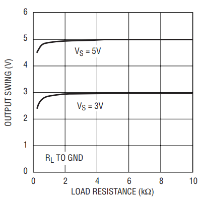
The LTC2050 maintains its DC characteristics while driving resistive loads requiring source or sink current as high as 5mA with a 3V or 5V supply. Figure 3 shows the op amp rail-to-rail swing versus output resistance loading. With a 1k or 5k load, the output typically swings to within 100mV or 30mV, respectively, of the rails.

Figure 3. LTC2050 output voltage swing vs load resistance.
Clock Feedthrough Virtually Eliminated
The LTC2050 uses autozeroing circuitry to achieve its zero-drift offset and other DC specifications. In the LTC2050, the clock used for autozeroing is typically 7.5kHz. The term clock feedthrough is used to indicate visibility of this clock in the op amp output spectrum. There are typically two types of clock feedthrough in autozeroed op amps such as the LTC2050.
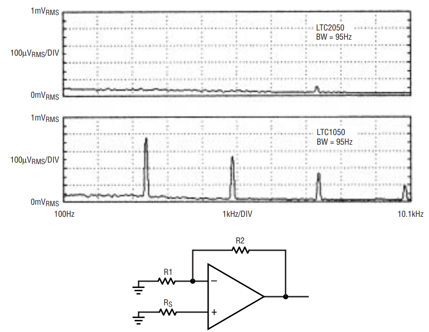
The first source is caused by the settling of the internal sampling capacitor and is input referred; that is, it is multiplied by the closed loop gain of the op amp. This form of clock feedthrough is independent of input source resistance or gain setting resistors. Figure 4 shows the spectrum of the LTC2050 with a closed loop gain of –100 with R2 = 100k, and R1 = RS = 1k. There is a residue clock feedthrough of less than 1µVRMS (input-referred) at 7.5kHz. This very low clock feedthough is achieved in the LTC2050 by internal circuitry that improves settling of the internal autozero storage capacitors. Also in Figure 4, the clock feedthrough of the LTC2050 is compared with that of the very popular LTC1050.

Figure 4. Output spectrum with a gain of 100; R2 = 100k; R1 = RS = 1k.
The second form of clock feedthrough appears when the input has a large source resistance or the gain setting resistors are large. In this case, the charge injection caused by the internal MOS switches creates input-referred clock feedthrough currents that are multiplied by the impedance seen at the input terminals of the op amp. This form of clock feedthrough is not significant in the LTC2050 when RS and R1 in Figure 4 are below approximately 10k. Placing a capacitor across R2 reduces either form of clock feedthrough by lowering the bandwidth of the closed-loop response.
Conclusion
The LTC2050 is the latest member of Linear Technology’s family of zero-drift operational amplifiers. It provides small packaging while still maintaining precision DC specifications. In addition, it operates at supplies as low as 2.7V and includes a power shutdown in the 6-lead SOT-23 package.


