LTC1668 DAC and LT1807 Op Amp Achieve 90ns Settling to 16 Bits and 83dB SFDR in a Small Footprint
LTC1668 DAC and LT1807 Op Amp Achieve 90ns Settling to 16 Bits and 83dB SFDR in a Small Footprint
2001-09-01
The LTC1668 is a new 16-bit, 50Msps differential, current output DAC in a small SSOP package. It has a 10mA full-scale output and a 1V output compliance and it achieves 20ns settling to 0.1% into 50Ω loads. The LT1807 is a 325MHz, 140V/µs precision, low noise dual op amp available in a small MSOP package. Its combination of precision, low noise, high bandwidth and fast slew rate make it ideal for high performance signal conditioning and acquisition systems. Together, these components create a fast, precise, versatile, low distortion VOUT DAC with minimal PCB space requirements.
The circuit in Figure 1 shows the LT1807 applied as a dual I/V converter to extend the LTC1668’s effective output compliance. With 200Ω feedback resistors (R1 and R2), the circuit gives output voltages of 0V to 2V or 4V differential. C8 and C9 are placed at the DAC outputs to roll off the bandwidth and reduce the step slew rate of the extremely fast DAC.

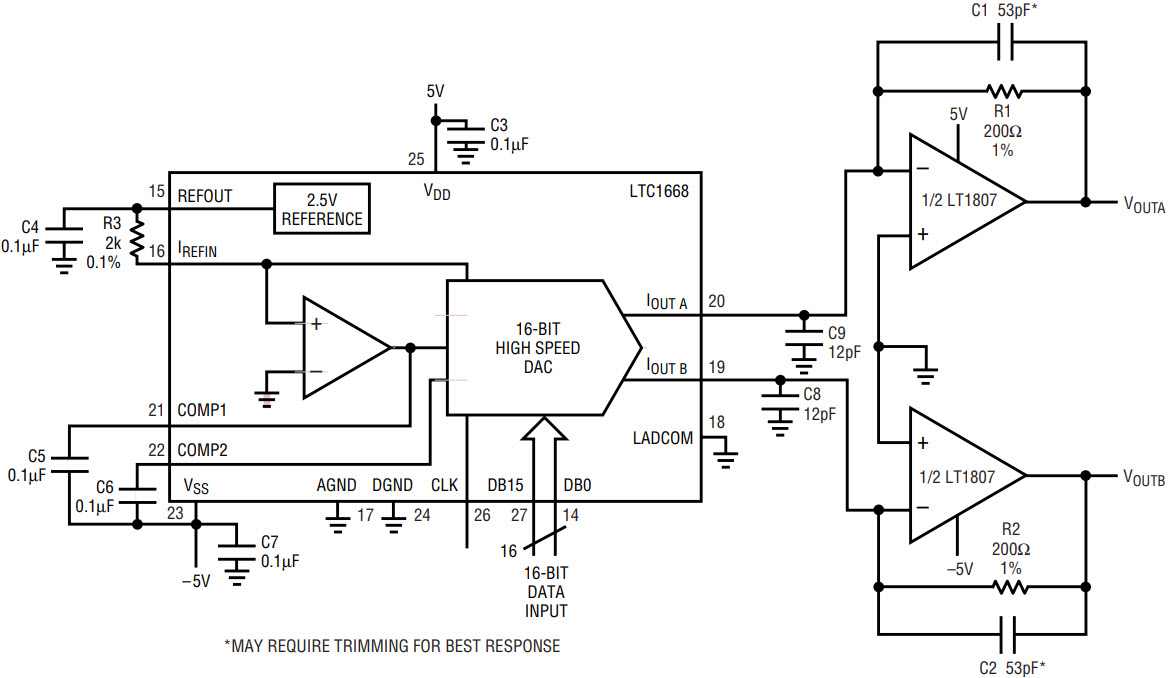
Figure 1. LTC1668 current output DAC followed by two 200Ω I/V converters using the LT1807.
The compensation capacitors C1 and C2 ensure stability and best possible settling time by canceling the pole that would otherwise be created by the total capacitance at the DAC outputs (parasitic and component). Output swings other than 0V to 2V can be achieved by selecting other values for R1 and R2 or by changing the DAC reference. The rail-to-rail outputs of the LT1807 allow designs with output swings approaching the upper supply rail.
With a 2V output swing, 16-bit resolution dictates an error band (±1LSB) of 60µV. We evaluated the circuit’s single-ended settling time according to the methods described in LTC Application Notes AN74 and AN79. The results are shown in Figure 2, with settling time measuring less than 90ns. Reducing the error band to ±1/2LSB moves the measured settling time out to just inside 120ns, at which point the effects of the transient are clearly finished. Persistence over a 500ns window was excellent but, although no longer settling tails were seen, the circuit was not intended or fully characterized for longer term 16-bit precision.

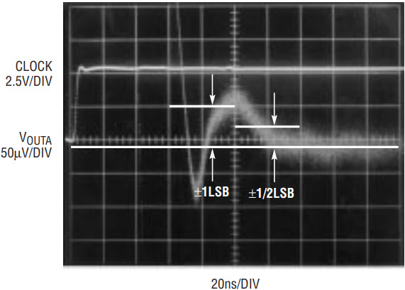
Figure 2. Settling-time measurement using the methods described in LTC Application Notes AN74 and AN79.
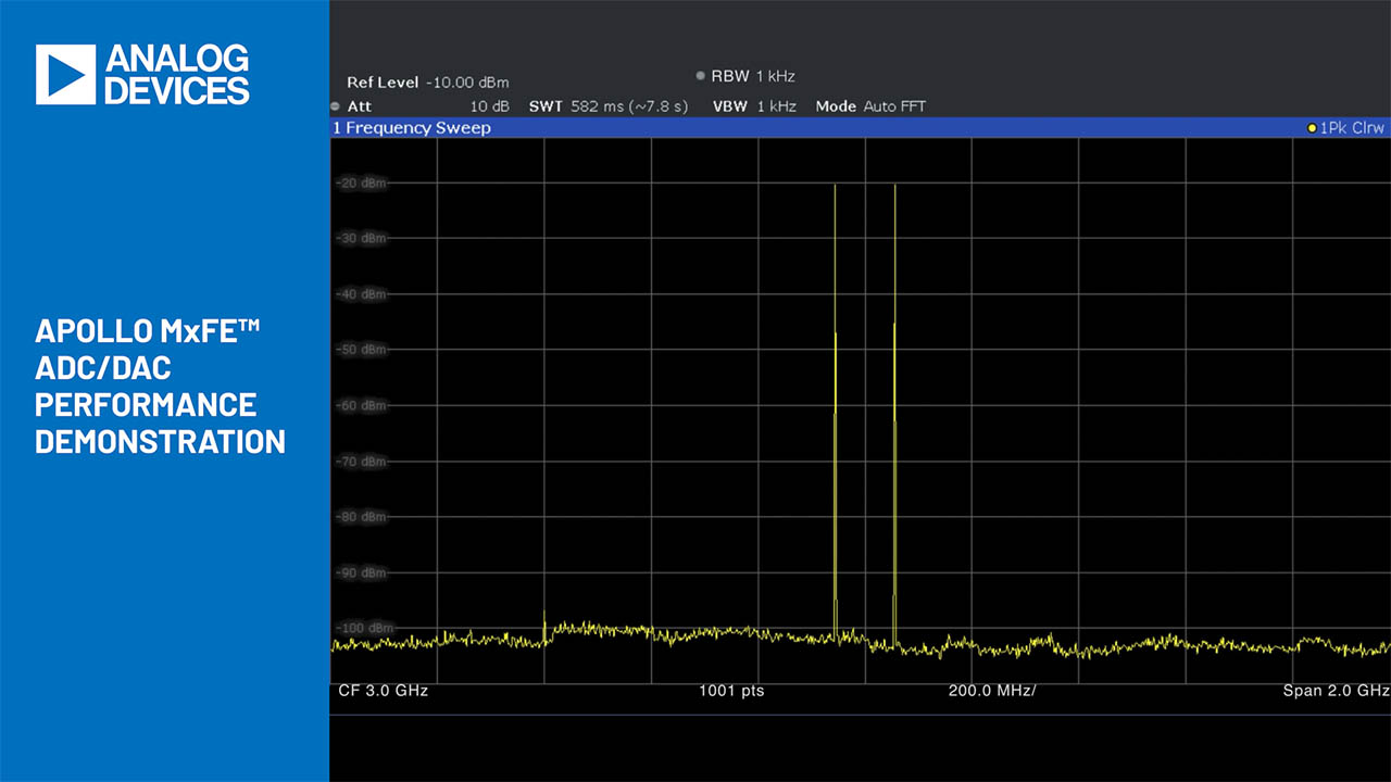
AC linearity of the circuit was measured operating with a sinusoidal output of 1MHz1 and a 25Msps clock. The results are shown in Figure 3, with the second harmonic down 83dB and the third harmonic down 86dB. The circuit’s DC linearity was measured at less than ±1LSB INL and DNL. Power consumption was measured at 30mA from the +5V supply and 50mA from the –5V supply, efficient for a DAC of this speed.

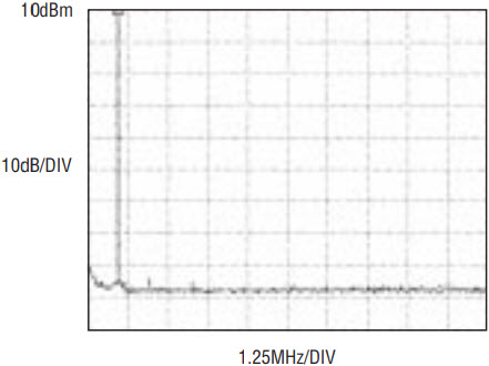
Figure 3. Frequency spectrum of 1MHz, 25Msps sinusoidal output shows 83dB SFDR.
Conclusion
The LT1807 and LTC1668 combine to make a small, fast, versatile and precise voltage output DAC. The excellent AC specifications make the circuit suitable for demanding waveform synthesis applications, whereas the fast settling and 16-bit resolution make it suitable for precise closed-loop control systems.
关于作者