Improve Hot Swap Performance and Save Design Time with Hot Swap Controller that Integrates 2A MOSFET and Sense Resistor
Improve Hot Swap Performance and Save Design Time with Hot Swap Controller that Integrates 2A MOSFET and Sense Resistor
by
David Soo
2009-06-01
Introduction
The LTC4217 Hot Swap controller turns a board’s supply voltage on and off in a controlled manner allowing the board to be safely inserted and removed from a live backplane. No surprise there, this is generally what Hot Swap controllers do, but the LTC4217 has a feature that gives it an advantage over other Hot Swap controllers. It simplifies the design of Hot Swap systems by integrating the controller, MOSFET and sense resistor in a single IC. This saves significant design time that would otherwise be spent choosing an optimum controller/MOSFET combination, setting current limits, and carefully designing a layout that protects the MOSFET from excessive power dissipation.
One significant advantage of an integrated solution over discrete solutions is that the current limit accuracy is well known. In discrete solutions, the overall precision of the current limit is a function of adding the tolerances of contributing components, while in the LTC4217, it appears as a single 2A specification.
The integrated solution also simplifies layout issues by optimizing MOSFET and sense resistor connections. The inrush current, current limit threshold and timeout can be set to default values with no external components or easily adjusted using resistors and capacitors to better suit a large range of applications. The part is able to cover a wide 2.9V to 26.5V voltage range and includes a temperature and current monitor. The MOSFET is kept in the safe-operating–area (SOA) by using a time-limited foldback current limit and overtemperature protection.
The LTC4217 can be easily applied in its basic configuration, or, with a few additional external components, set up for applications with special requirements.
Monitoring the MOSFET
The LTC4217 features MOSFET current and temperature monitoring. The current monitor outputs a current proportional to the MOSFET current, while a voltage proportional to the MOSFET temperature is available. This allows external circuits to predict possible failure and shutdown the system.
The current in the MOSFET passes through a sense resistor, and the voltage on the sense resistor is converted to a current that is sourced out the IMON pin. The gain is 50µA from IMON for 1A of MOSFET current. The output current can be converted to a voltage using an external resistor to drive a comparator or ADC. The voltage compliance for the IMON pin is from 0V to (INTVCC – 0.7V).
The MOSFET temperature corresponds linearly to the voltage on the ISET pin, with the temperature profile shown in Figure 1. The open circuit voltage on this pin at room temperature is 0.63V. In addition, the overtemperature shutdown circuit turns off the MOSFET when the controller die temperature exceeds 145°C, and turns it on again when the temperature drops to 125°C.
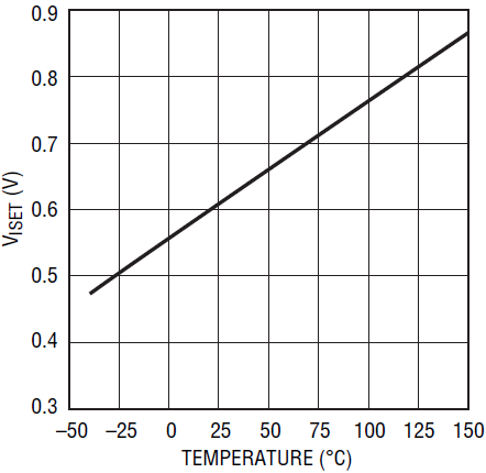
Figure 1. VISET vs temperature
12V Application
Figure 2 shows the LTC4217-12 in a 12V Hot Swap application with default settings. The only external component required is the capacitor on the INTVCC pin. The current limit, inrush current control, and protection timer are internally set at levels that protect the integrated MOSFET. The input voltage monitors are preset for a 12V supply using internal resistive dividers from the VDD supply to drive the UV and OV pins. The UV condition occurs when VDD falls below 9.23V; OV when VDD exceeds 15.05V.
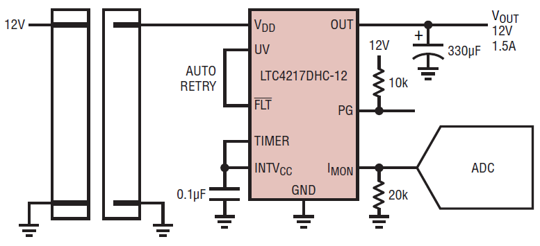
Figure 2. 12V, 1.5A card resident application
The LTC4217 turns a board’s supply voltage on and off in a controlled manner, allowing the board to be safely inserted and removed from a live backplane. Several conditions must be present before the internal MOSFET can be turned on. First the VDD supply exceeds its 2.73V undervoltage lockout level and the internally generated INTVCC crosses 2.65V. Next the UV and OV pins must indicate that the input power is within the acceptable range. These conditions must be satisfied for the duration of 100ms to ensure that any contact bounce during the insertion has ended.
The MOSFET is then turned on by a controlled 0.3V/ms gate ramp as shown in Figure 3. The voltage ramp of the output capacitor follows the slope of the gate ramp thereby setting the supply inrush current at:

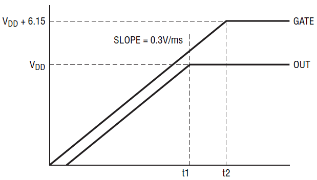
Figure 3. Supply turn-on
To reduce inrush current further, use a shallower voltage ramp than the default 0.3V/ms by adding a ramp capacitor (with a 1k series resistor) from gate to ground.
As OUT approaches the VDD supply, the powergood indicator (PG) becomes active. The definition of power good is the voltage on the FB pin exceeds 1.235V while the GATE pin is high. The FB pin monitors the output voltage via an internal resistive divider from the OUT pin. Once the OUT voltage crosses the 10.5V threshold and the GATE to OUT voltage exceeds 4.2V, the PG pin ceases to pull low and indicates that the power is good. Once OUT reaches the VDD supply, the GATE ramps until clamped at 6.15V above OUT.
The LTC4217 features an adjustable current limit with foldback that protects against short circuits or excessive load current. The default current limit is 2A and can be adjusted lower by placing a resistor between the ISET pin and ground. To prevent excessive power dissipation in the switch during active current limit, the available current is reduced as a function of the output voltage sensed by the FB pin as shown in Figure 4.
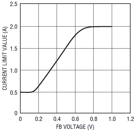
Figure 4. Current limit threshold foldback
An overcurrent fault occurs when the current limit circuitry has been engaged for longer than the delay set by the timer. Tying the TIMER pin to INTVCC configures the part to use a preset 2ms overcurrent time-out and a 100ms cool-down time. After the 100ms cool-down, the switch is allowed to turn on again if the overcurrent fault has been cleared. Bringing the UV pin below 0.6V and then high clears the fault. Tying the FLT pin to the UV pin allows the part to self-clear the fault and turn on again after the 100ms cool-down.
Programmable Features
The LTC4217 application shown in Figure 5 demonstrates the adjustable features.
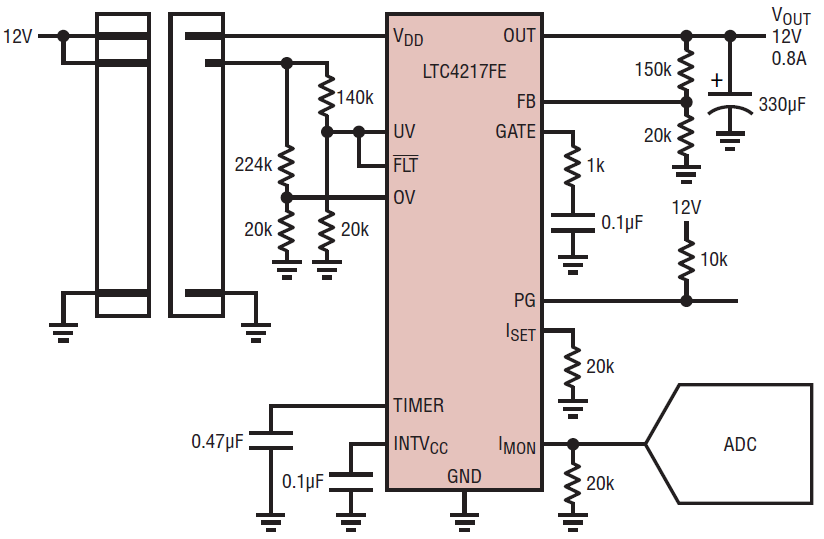
Figure 5. 0.8A, 12V card resident application
The UV and OV resistive dividers set undervoltage and overvoltage turnoff thresholds while the FB divider determines the power good trip point. The R-C network on the GATE pin decreases the gate ramp to 0.24V/ms from the default 0.3V/ms to reduce the inrush current.
The 20k ISET resistor forms a resistive divider with an internal 20k resistor to reduce the current limit threshold (before foldback) to one-half of the original threshold for a 1A current limit. The graph in Figure 6 shows the current limit threshold as the ISET resistor varies.
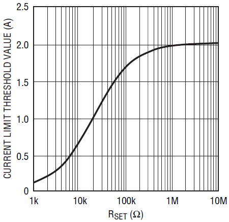
Figure 6. Current limit adjustment
As in the previous application, the UV and FLT signals are tied together so that the part auto-retries turn-on following shutdown for an overcurrent fault.
This example places a 20k resistor on the IMON pin to set the gain of the current monitor output to 1V per amp of MOSFET current.
Instead of tying the TIMER pin to the INTVCC pin for a default 2ms overcurrent timeout, an external 0.47µF capacitor is used to set a 5.7ms timeout. During an overcurrent event the external timing capacitor is charged with a100µA pull-up current. If the voltage on the capacitor reaches the 1.2V threshold, the MOSFET turns off. The equation for setting timing capacitor’s value is as follows:

While the MOSFET is cooling off, the LTC4217 discharges the timing capacitor. When the capacitor voltage reaches 0.2V an internal 100ms timer is started. Following this cool down period the fault is cleared (when using auto-retry) and the MOSFET is allowed to turn on again.
It is important to consider the safe operating area of the MOSFET when extending the circuit breaker timeout beyond 2ms. The SOA graph for the MOSFET used in LTC4217 is shown in Figure 7. The worse case power dissipation occurs when the voltage versus current profile of the foldback current limit is at maximum. This occurs when the current is 1A and the voltage is one half of the 12V or 6V (see Figure 4, FB pin at 0.7V). In this case the power is 6W, which dictates a maximum time of 100ms (Figure 7, at 6V and 1A).
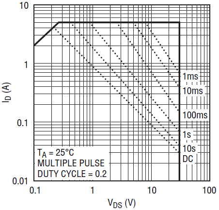
Figure 7. MOSFET SOA curve
Conclusion
The primary role of the LTC4217 is to control hot insertion and provide the electronic circuit breaker function. Additionally the part includes protection of the MOSFET with focus on SOA compliance, thermal protection and precise 2A current limit. It is also adaptable over a large range of applications due to adjustable inrush current, overcurrent fault timer and current limit threshold. A high level of integration makes the LTC4217 easy to use yet versatile.


