High Speed SO-8 12-Bit ADCs Run on 5V or 3V
Introduction
Advancing the leading edge of high speed, low power 12-bit serial ADCs in SO-8, LTC introduces the LTC1401 and LTC1404. The LTC1401 is a single 3V supply, 200ksps 12-bit ADC. The LTC1404 is a pin-to-pin compatible upgrade of the existing LTC1400. It samples at 600ksps on either single 5V or ±5V supplies. Both of these devices are small in size but big in features. They achieve speeds that are far ahead of the pack. Once again, LTC has rewritten the record for the highest throughput per square area of board space of any 12-bit ADC on the market. Both devices satisfy tomorrow’s digitally based signal-processing requirements while achieving a minimum footprint.
Full ADC Features in an SO-8 Package
3V, 5V or ±5V Supplies
The LTC1401 provides a complete 200ksps unipolar A/D solution operating on a single supply as low as 2.7V. The typical supply current is 5mA and the analog input range is from 0V to 2.048V, yielding an LSB of 0.5mV. Unlike the LTC1400 and LTC1404, the unipolar LTC1401 replaces the unused negative supply pin with a power-down input. The user can power the chip down immediately by pulling this pin low. Like the LTC1400, the LTC1404 operates on a single 5V or ±5V supplies and consumes about 15mA. The analog input signal range is automatically determined by the supply voltage. If VSS is connected to ground, the chip operates in unipolar mode and accepts analog signals between 0V and 4.096V. If VSS is connected to a –5V supply, the chip enters bipolar mode, in which case the input range is ±2.048V. In either mode, the LSB is 1mV. Figure 1 shows a typical application for LTC1401 or LTC1404.

Figure 1. LTC1401 and LTC1404 typical applications.
Reference, S/H and Serial I/O
The common features shared by both devices include a precision internal reference, which can be overdriven externally, and high frequency S/H circuitry. The high impedance analog input can be driven through a MUX without adding any DC errors due to on-resistance. The low input capacitance allows fast acquisition time for the sample-and-hold, even with high source impedance. There is a simple 3-wire digital interface to the host computer, DSP or microcontroller. The interface consists of a serial input clock (CLK), data output (DOUT) and a convert-input start (CONV) signal. The CONV input allows precise control of each sample conversion, so vital to DSP applications that require precise sampling. The rising CLK edge synchronizes all the ADC events to make sure that none of the ADC’s critical comparisons occur simultaneously with a clock edge or data-out transition. The DOUT pin is at high impedance when the ADC is not converting. During operation, it first pipes out a REFRDY bit and follows this with the 12-bit serial data. Figure 2 shows the block diagram and the digital timing. The block diagram illustrates the pinout and functional differences between the LTC1401 and LTC1404. The REFRDY bit indicates that the internal reference is ready for conversion. REFRDY is a logic 1 if the reference is valid; otherwise it outputs a 0. This bit indicator becomes a very useful feature when the chip is toggling between the active and power-down modes.
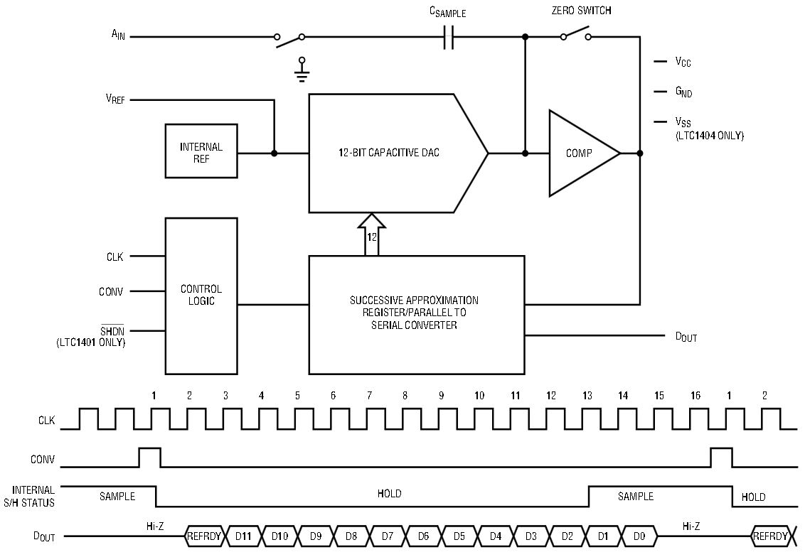
Figure 2. Block and timing diagrams.
NAP and SLEEP Shutdown Modes
The combination of CLK and CONV signals serves another very important function. The ADCs can be placed in NAP or SLEEP mode with the proper manipulation of these two input signals. Figure 3 shows the power-down timing waveform. With CLK held at a logic low, two consecutive CONV pulses activate NAP mode and shut down all internal circuitry except the reference, which fully charges the external bypass capacitor; the REFRDY bit is high. Under this condition, the supply currents for the LTC1401 and LTC1404 are 500µA and 1.3mA, respectively. Either ADC can be reawakened quickly to resume conversion. If the ADC is not reawakened and CLK is still held low, another two consecutive CONV pulses (a total of four pulses) activate the SLEEP mode and shut down the reference; the charge on its bypass capacitors goes to zero and the REFRDY bit goes low, reducing the supply current to 6.5µA for the LTC1401 and 8µA for the LTC1404. Figure 4 shows the power supply consumption of the LTC1404 in its various operating modes.
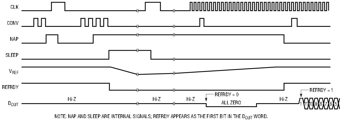
Figure 3. NAP and SLEEP mode waveforms.
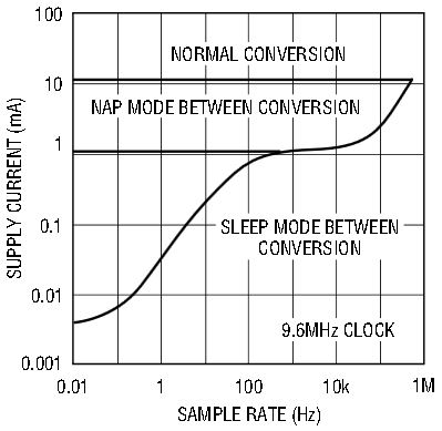
Figure 4. LTC1404 power consumption invarious operating modes.
Reference Ready Indicator
In NAP or SLEEP mode, the first rising CLK edge returns the ADC to normal operation. When SLEEP is deactivated on the LTC1404, the internal reference is first powered up and the reference capacitor is slowly charged. Since the LTC1404 has limited source-current capability to charge the capacitor, a finite time is needed and this time depends on the capacitance value. Guesswork as to when the capacitor is fully charged is eliminated by monitoring the REFRDY bit. The REFRDY bit guarantees that the reference is steady and the digital result is correct. Some competing ADCs need an off-chip reference. With these parts, it is up to the system designer to come up with a way to put the reference to sleep and to determine just how long it takes to wake up. Because of board-level variations or varying reference loading conditions, the converted output may not be correct because of different reference wake-up times. With their proprietary power-down scheme, the high speed LTC1401 and LTC1404 can save more power when operating at low sampling rates than some “micropower” ADCs without a power-down feature.
Easy to Apply
Ground Plane
As with other high resolution, high speed ADCs, the LTC1401/LTC1404 needs some basic attention to layout details. These include grounding, bypassing and lead inductance. The best performance is achieved when the LTC1401/LTC1404 is applied as an analog device and powered from an analog supply. Its ground pin should be connected to an analog ground plane. This ground plane should have only one connection to the system ground. This prevents system-ground currents from taking a short cut through the analog ground. This single connection should be made to a point near the ADC ground pin. Alternatively, a 10Ω resistor or a ferrite bead jumper instead of a direct short may help to reduce the digital noise.
Supply Bypassing
Noise on the power supply can cause ADC errors. At low frequencies, the converter has very good power supply rejection, but as frequency increases, all converters lose the ability to reject power-supply noise. To eliminate power-supply noise, the LTC1401/LTC1404 VCC pin should be bypassed directly to the analog ground plane with a good 10µF AVX capacitor in parallel with a 0.1µF ceramic; for better results, another 10µF AVX capacitor can be added. At 600ksps, the LTC1404’s CLK frequency can be as high as 9.6MHz. Some poor quality capacitors can lose more than 80% of their capacitance in this frequency range. Therefore, it is important to consult the manufacturer’s data sheet before selecting a capacitor. For the LTC1404, at 600ksps, every bit decision must be determined within 104ns (9.6MHz). During this short time interval, the supply disturbance due to CLK transition must settle, the ADC must update its DAC, make a comparator decision, latch the new DAC information and output the serial data. Both of these ADCs have only one power supply pin, which is connected to both the internal analog and digital circuitry. Any ringing due to poor bypassing, parasitic trace inductance, CLK and CONV over/undershoot or unnecessary DOUT current loading can cause ADC errors. Narrow power supply traces should be avoided. Their comparatively high inductance can lead to compromised bypass performance and conversion errors. The input signals for the CLK and CONV pins should be terminated properly. The DOUT signal should be buffered if necessary to drive a long trace or heavy load.
DC and AC Performance
With these basic concerns in mind, it is not difficult to obtain the best performance from the LTC1401 and LTC1404. The DC performance of the LTC1401 and LTC1404 includes ±1LSB INL and DNL. No missing codes are guaranteed over temperature. In addition to these excellent DC specifications, these devices have curvature-corrected 1.20V (LTC1401) or 2.43V (LTC1404) precision references. For high frequency conversion applications, the LTC1401 and LTC1404 excel, with outstanding AC performance. Figures 5 and 6 show the performance of the LTC1401 and LTC1404, respectively.
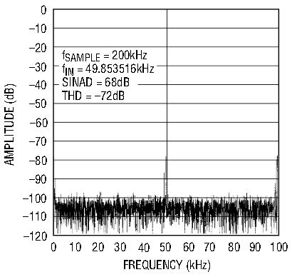
Figure 5a. LTC1401 FFT.
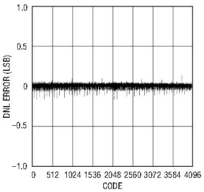
Figure 5b. LTC1401 DNL error.
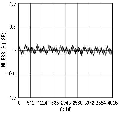
Figure 5c. LTC1401 INL error.
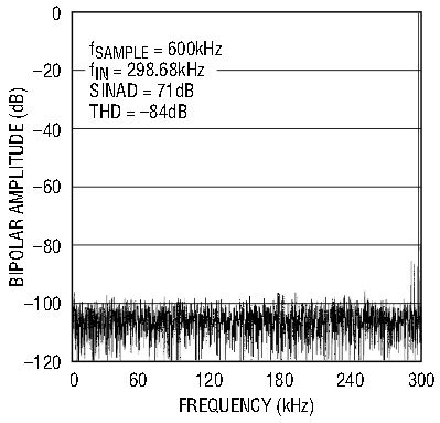
Figure 6a. LTC1404 FFT.
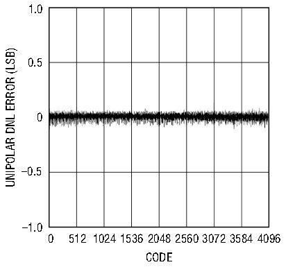
Figure 6b. LTC1404 DNL error.
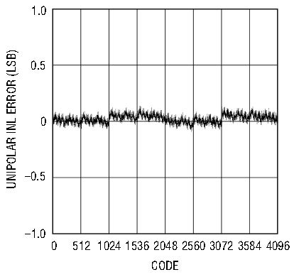
Figure 6c. LTC1404 INL error.
Applications
The LTC1401 and LTC1404 will find applications in telecommunications, digital signal processing, portable-computer data acquisition boards and high speed or multiplexed data acquisition.
In telecommunication applications such as HDSL (high-bit-rate digital subscriber line interface), high speed and low power dissipation are a must because the systems are usually powered by the phone line itself. Excellent dynamic performance is required of the ADC’s sample-and-hold. The serial interface minimizes the number of signal lines that must be routed, thereby saving significant board space. The 600ksps LTC1404, with its SO-8 footprint, is an excellent choice for HDSL applications. At 584ksps, with 2B1Q coding, the LTC1404 receives at 2.048Mbps over two wires.
Another common use of ADCs is in data acquisition applications. System designers have always faced problems in optimizing data acquisition applications for speed, size, power and cost, especially in the case of portable designs. The high sample rate, the high level of functional integration and the low cost of these converters make them ideal choices for these applications. The LTC1401 and LTC1404 can be easily interfaced to a low cost MUX (for example, a CD4051, 74HC4051 or LTC1391) through their high impedance inputs. The high input impedance of these ADCs eliminates the need for a buffer between the MUX and the ADC, resulting in savings of both cost and board space.
Conclusion
The new LTC1401 and LTC1404 come with full ADC performance and an easy-to-use serial interface. These complete, stand alone, high speed, low power devices will simplify the job of system designers.


