Dual Hot Swap Controller Brings Digital Monitoring to AdvancedTCA, µTCA and AMC Applications
Dual Hot Swap Controller Brings Digital Monitoring to AdvancedTCA, µTCA and AMC Applications
2009-01-01
Introduction
Recently ratified plug-in card bus standards, such as AdvancedTCA, µTCA and AMC, reduce the number of power supplies that are routed across the connector when compared to earlier standards, such as CompactPCI. Bulk power is limited to one fairly high voltage supply, making for an efficient distribution channel. For instance, distributed 12V power is locally converted to lower voltages to minimize distribution currents and related losses in connectors and power handling circuitry. Some cards also have a lower voltage (3.3V) maintenance power supply that provides low current housekeeping functionality to a card even when the bulk supply is off.
Even with the obvious simplification that these standards bring, there remain rigorous power, heat dissipation and reliability requirements, which demand advanced Hot Swap, monitoring and control capability. The LTC4222 satisfies these requirements with dual Hot Swap controllers and integrated voltage and current monitoring via an onboard ADC.
Hot swapping requires a power switch to initially isolate the board, and a controller to slowly turn on the switch to minimize backplane disturbances. Since the Hot Swap controller monitors card voltage and current, it is a natural place to integrate higher level monitoring with a data converter. This provides detailed information about the health of the power path and the power consumption of down-stream circuits. Such information can be used to monitor performance over time and identify boards that are drifting towards failure or out of spec.
The LTC4222 works in applications from 24V (with transients to 35V) down to 3.3V where the operating input voltage could drop to 2.9V. Functionally, the LTC4222 is very similar to a pair of LTC4215s or LTC4260s. Table 2 compares features of the LTC4222, LTC4215 and LTC4260. Since all three parts may be used for 12V systems, Table 2 may be used to select the part(s) with the optimal set of features for a specific 12V application.
| Feature | Benefits |
| Wide Input Voltage Range: Operates from inputs of 2.9V to 29V, with 35V absolute maximum |
❏ Suitable for 3.3V, 5V, 12V and 24V systems ❏ Simplifies design because part functions on a semi-regulated supply ❏ Large overvoltage transient range eases design tolerances for transient protection |
| 10-Bit ADC: Monitors current, output voltage and external pin voltage |
❏ Increases reliability ❏ Board power information provides an early warning of board failure ❏ Verify board is staying within its allotted power ❏ Allows integrity check of redundant supply paths ❏ Allows active power management to safely maximize power utilization within the chassis cooling constraints |
| I2C/SMBus: Communicates as a read-write slave device using a 2-wire serial interface |
❏ Improves integration with the host system. Interface allows the host to configure the part, determine which faults are present or have occurred, and read back ADC measurements |
| Optionally Coupled Faults: The config pin allows channels to function independently or couples faults to shut down both channel if either generates a fault |
❏ Provides flexibility for different architectures ❏ Allows the part to power two independent sockets or sequence the application of power ❏ Enables both channels to shut down on a fault, isolating a faulty board |
| Fast short Circuit Response: Fast (<1µs) current limit response to shorts |
❏ Protects connector from overcurrent ❏ Limits the disturbance to the input supply from a short circuit |
| Alert Host After Faults: When configured (using I2C), faults activate an active pull-down on the ALERT pin |
❏ Interrupting the host for immediate fault servicing limits system damage ❏ Reduces the bus traffic for polling |
| Feature | LTC4222 | LTC4215 | LTC4260 |
| Channels | 2 | 1 | 1 |
| VDD Abs Max | 35V | 24V | 100V |
| VDD Min | 2.9V | 2.9V | 8.5V |
| Current Limit/Circuit Breaker | 50mV | 25mV | 50mV |
| Circuit Breaker Precision | 5% | 10% | 10% |
| Built in Overvoltage Threshold | 15.6V | ||
| Optional Coupled Faults |  |
||
| ADC Direct Address/Alert |  |
||
| ADC Resolution | 10-bit | 8-bit | 8-bit |
| ADC SOURCE LSB | 31.25mV | 60mV | 400mV |
| ADC VSENSE LSB | 62.5µV | 151µV | 300µV |
| ADC ADIN LSB | 1.25mV | 4.85mV | 10mV |
| Internally Generated VCC | 3.3V | 3.1V | 5.5V |
| Package | 5mm × 5mm QFN | 4mm × 5mm QFN | 5mm × 5mm QFN |
AMC Application
The LTC4222 combines a robust Hot Swap circuit with a data converter and I2C interface to allow power monitoring in addition to hot plug functionality and fault isolation. In a typical application, see Figure 1, the LTC4222 uses external N-channel pass transistors to isolate the hot swapped board from the backplane when it is first inserted. After a debounce time the controller can begin to apply power to the board or wait for a turn-on command from a host processor. Power is gradually ramped up to minimize any backplane disturbance. After the power-up process is complete, the LTC4222 continues to monitor for faults in the power path. The CONFIG pin controls whether the two channels start-up and turn-off at the same time or independently. Some of the major features of the LTC4222 are listed in Table 1.
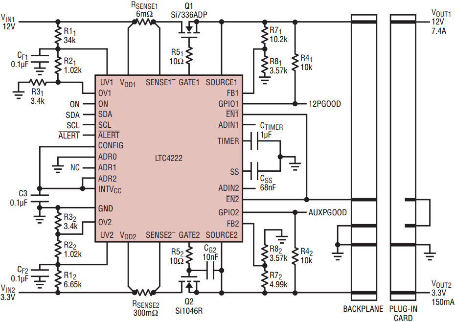
Figure 1. Typical AMC application.
An N-channel pass transistor, Q1, controls the application of power to VOUT1 on the board as in Figure 1. A series sense resistor, RSENSE, allows the LTC4222 to measure the current in the power-path with the ADC and provides the current sense input to the current limit and circuit breaker. Resistor R5 suppresses self-oscillations in Q1. Resistors R1–R3 set the undervoltage (UV) and overvoltage (OV) fault thresholds. Capacitor CF filters the power signal to prevent faults from noise or transient events. R7 and R8 select the power good threshold and set the foldback current limit level, which dramatically improves safe operating area (SOA) requirements for Q1. Capacitor CSS sets a maximum inrush current slew rate to avoid transient glitches on the backplane and CTIMER is used to set the start-up time limit, which protects Q1 by turning it off if the system attempts to start-up into an excessive load. C3 is used to bypass the internal 3.3V core voltage on the INTVCC pin and prevent the LTC4222 from resetting on input supply glitches. The INTVCC pin may also be used to power external loads, such as an I2C bus buffer, up to 10mA. The behavior of channel 2 is identical to channel 1.
Typically, the pins on the connector are staggered so that bulk power is applied first with the longest pins, followed by communication lines on medium length pins, and finally, Hot Swap control lines such as the supply for the UV, OV, or EN pins. The UV, OV, and EN pins must be in the correct state for a period of 100ms before Q1 is allowed to turn on to allow any connector signal bouncing to subside before starting up. At this point the ON pin turns the part on immediately if it is high, or holds the part off if it is low. The ON pin can be overridden and Q1 turned on or off through the I2C bus by writing to the ON bit in the control register.
If the CONFIG pin is low, these conditions must be met for both channels to initiate start-up, and both channels will start up at the same time, as shown in Figure 2. A fault on either channel when the CONFIG pin is low results in both channels turning off, as shown in Figure 3, at which point they latch off or auto-retry together as configured in the control registers. This allows a faulting board to be entirely disconnected.
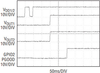
Figure 2. Start-up waveform with coupled turn-on.
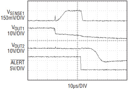
Figure 3. Fault-off waveform with coupled faults.
When the CONFIG pin is tied high, the two channels can start-up independently as long as both VDD voltages are above their UVLO levels. If one channel is enabled during the 100ms debounce time of the other channel, the 100ms debounce is restarted and both channels will start together, however if one channel is enabled while the other channel is starting up or going through an overcurrent cool-down cycle, the channel attempting to start must wait for the other channel to finish before it is allowed to start.
With CONFIG tied high, the two channels can easily be sequenced by tying the power good output on the GPIO pin of one channel to the UV pin of the other channel. The GPIO pin pulls down the UV pin and holds the other channel off until the first channel starts up and the FB pin detects that power is good, at which point the GPIO pin releases the UV pin and the second channel starts up, as shown in Figure 4.
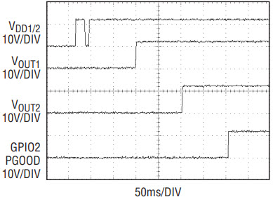
Figure 4. Start-up waveform with sequencing.
If one channel experiences a fault when the CONFIG pin is tied high, the other channel remains on, as shown in Figure 5. This allows the LTC4222 to supply two slots on a backplane-based application where non-failing slots are supposed to remain on when adjacent slots fail, such as providing 12V payload power switching for two µTCA slots as shown in Figure 6.
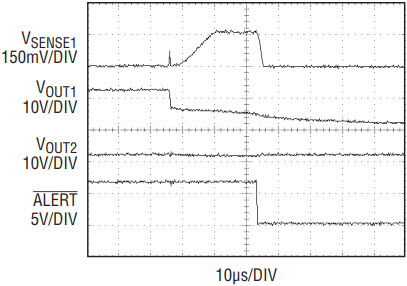
Figure 5. Fault-off waveform with independent faults.
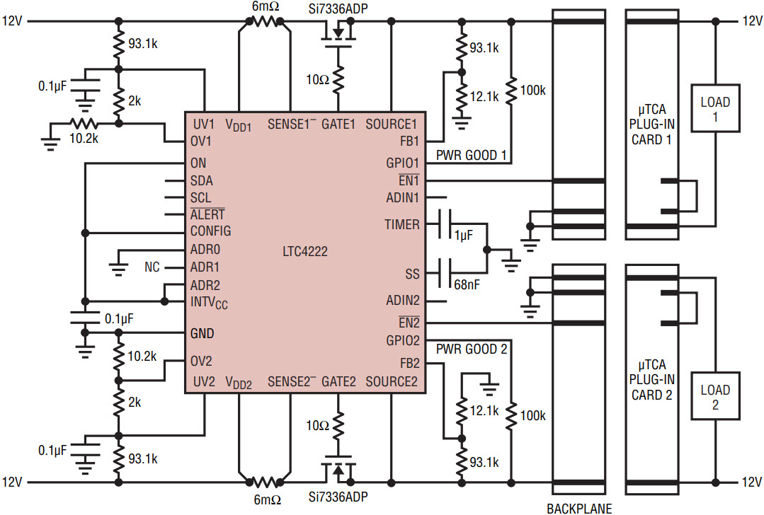
Figure 6. µTCA application supplying 12V payload power to two µTCA slots.
Measure Board Power with Integrated ADC
Monitoring the supply voltage and current is a useful way of tracking the health of the power path. New data can be compared with historical data for the same card to detect changes in power consumption that could indicate that the card is behaving abnormally. An abnormal card can be shut down and flagged for service, perhaps before a more severe fault or system malfunction occurs. The LTC4222 includes a 10-bit data converter that continuously monitors six voltages: two ADIN pins, two SOURCE pins and two current sense voltages between the SENSE+ and SENSE– pins. The ADIN pins are uncommitted ADC inputs that allow the user to monitor any available voltage. The ADIN pins are monitored with a 1.28V full scale and are connected directly to the data converter input without any signal scaling. The SOURCE pins use a 1:24 divider at the input, which gives a 32V full scale. The SENSE voltage amplifiers have a voltage gain of 20, which results in a 64mV full scale. The converter uses an over-sampling and offset cancellation method that preserves the full 10-bit dynamic range on the SENSE channels.
If the data converter reads more than 2mV on a VDD–SENSE channel while the external switch is turned off, the LTC4222 generates a FET-SHORT fault to indicate that the switch may be damaged. The presence of this condition is indicated in the STATUS register bit C5 for the originating channel and logged to FAULT register bit D5. The LTC4222 takes no action in this condition other than logging the fault and generating an alert if configured to do so.
The results from each conversion are stored in 12 ADC registers. The default behavior of the data converter is a free-running mode in which it sequentially measures all six channels continuously and updates the output registers 15 times per second. The data converter can be stopped by setting ADC_CONTROL register bit 0 (HALT)—subsequent writes to the ADC_CONTROL register with the HALT bit set initiate a single conversion on the data converter channel selected by ADC_CONTROL register bits 1–3. An optional alert can be generated on the ALERT pin to indicate a conversion has finished by setting ADC_CONTROL register bit 4, or alternately the ADC_BUSY bit (ADC_CONTROL bit 5) can be polled until it indicates that the data converter has completed the conversion. Note that the ADC_BUSY bit is always set when the data converter is in its free-running mode. When the data converter is halted, the data converter registers may be written to and read from for software testing.
Versatile Inrush Current Control
As described above, the LTC4222 waits to turn on each channel’s external switch until the channel’s input has met the UV and OV thresholds and an internal 100ms debounce timer has expired. The start-up time is determined by the capacitor on the TIMER pin, or 100ms if the TIMER pin is tied to INTVCC. During this time the circuit breaker is disabled to prevent an overcurrent fault from occurring, the power good signal from the corresponding GPIO pin is also disabled to prevent turning on a load before the current limit has reached the full value via the SS (soft-start) and FB (foldback) pins. The inrush current slew rate (dI/dt) is limited via the SS pin. The inrush current is also folded back from 50mV to 17mV via the FB pin. An optional RC network on the external MOSFET gate can be used to set the inrush current below the foldback level by setting the maximum slope of the output voltage. When both channels are starting up at the same time, the current sense voltages are both regulated to the lowest value commanded by the two FB pins and the SS pin.
At the end of the start-up period the current limit circuit is checked. If the current limit is still regulating the current, the LTC4222 determines that the output failed to come up and generates an overcurrent fault. If the current limit circuit is not active then the current limit threshold is moved to 150mV, the power good signal to the GPIO pin is enabled and the 50mV circuit breaker is armed.
The SS pin sets the current slew rate limit at start-up. It starts at ground, which corresponds to a negative voltage on the sense resistor and results in the MOSFET being turned off. A current into the soft-start capacitor produces a ramp that corresponds to increasing VDD–SENSE voltage. When either channel’s current limit circuit releases the gate (when the commanding VDD–SENSE voltage becomes positive) the current from the SS pin is stopped to wait for that GATE pin to rise and start to turn on the MOSFET.
Once the current limit circuit begins to regulate the VDD–SENSE voltage, the current from the SS pin is resumed and the ramp continues until it reaches the foldback level. It is important that the SS pin stop the ramp while the GATE pins are slewing because the ramp would otherwise continue and result in an uncontrolled step in current once the MOSFET threshold is reached. An uncontrolled step may violate inrush specifications and cause supply glitches on the backplane. Due to offset differences between the current limit circuits, the soft-start ramp may pause twice as each gate slews at a different time when both channels turn on in the same start-up cycle.
If the soft-start ramp reaches one of the the foldback current limit levels, the soft-start circuit stops the ramp. The ramp is allowed to continue as the voltage at the lowest FB pin rises and increases the foldback current limit, still limited in slope and limited in magnitude by foldback as well. The FB pin for a channel that is either on or off while the other is starting up is ignored and does not affect the startup current limit.
If an RC network is placed on a GATE pin to manually set the inrush current to a value below the foldback level, the current limit circuit leaves regulation and begins slewing when it is unable to achieve the VDD–SENSE voltage commanded by the SS and FB pins. If the start-up timer expires in the meantime, an overcurrent fault is not generated because the current limit is not active. The power good output for the GPIO pin relays the state of the FB pin, and the circuit breaker is armed. Either the output voltage finishes rising and a power good is asserted when the FB pin crosses it’s 1.235V threshold, or the current rises to the circuit breaker threshold and the part generates an overcurrent fault.
In the event there is an overcurrent condition after start-up, the current limit circuit limits the VDD–SENSE voltage to 150mV while the circuit breaker waits for a 20µs timeout before producing an overcurrent fault. After any overcurrent fault, the part waits for a cool-down period of 50 times the start-up time before allowing either channel to start or restart via auto-retry, or cycling the EN, UV or OV pins. The ON pins or the ON bits in the control registers can be cycled to bypass the cool-down time.
Controlled Turn-Off
When the LTC4215 is turned off by a fault or I2C transaction, the GATE pin is pulled down with a 1mA current source. Once the GATE pin is below the SOURCE pin, a diode from SOURCE to GATE turns on and the voltage at the SOURCE pin is discharged by the same 1mA current.
If there is a short that causes the sense voltage to exceed 150mV, a 450mA pull-down current from GATE to SOURCE removes the gate charge of the switch. Once the sense voltage falls to 150mV, the current limit regulates there for 20µs before turning the gate off with the 1mA current source.
If there is a significant inductance between VDD (SENSE+) and upstream bulk capacitance, across a connector for instance, it is possible that a short circuit at the output with a very fast discharge time could cause the VDD input voltage to collapse while the current through this inductance slews. In this case, after 2µs, the VDD undervoltage lockout circuit turns on and discharges the GATE pin with the 450mA pull-down to the SOURCE pin to quickly turn the switch off.
Save Power with Precise 50mV Circuit Breaker
In systems where a circuit breaker has only 20% accuracy, the designer must be able to safely provide 50% more power than the card actually consumes to ensure that the application doesn’t suffer from heat and supply limitations on the high side or produce a fault in normal operation on the low side. For instance, in a system that requires 10A, a 20% accurate hot swap must have a nominal circuit breaker threshold of 12.5A. Since the threshold could be as high as 15A, the power supply needs to be able to supply 15A. In the case of a 5% threshold, the nominal threshold is 10.5A and the maximum possible current is 11A. Using the part with a 5% circuit breaker over the part with the 20% circuit breaker frees 4A for use elsewhere, or allows the use of a 30% smaller, and less expensive, power supply.
High Voltage Rating for 12V Applications
The LTC4222 has a maximum input voltage rating of 35V, which is higher than the breakdown voltage of the external MOSFET for most 12V applications, and also allows the LTC4222 to be used in 24V applications. If the breakdown voltage of the external MOSFET is less than the 35V abs-max of the LTC4222, there is no need for a transorb at the input in a card-resident application because voltage surges are safely absorbed by the MOSFET. If a transorb is still required, the high voltage rating of the LTC4222 makes it easy to select a transorb above the maximum operating range of the application, and below the 35V maximum for the part.
Conclusion
The LTC4222 is a smart power gateway for boards with two or more hot-swappable supplies. It provides fault isolation, closely monitors the health of the power paths and provides versatile means of controlling the inrush current profile. It logs faults, provides real-time status information, and can interrupt the host if necessary. Meanwhile, an internal 10-bit ADC continuously monitors board current and voltages. These features make the LTC4222 an ideal power gateway for high availability systems.


