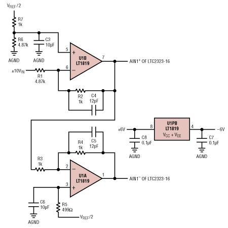
Here is a driver circuit for the LTC2323-16 dual 16-bit differential input ADC. This circuit accepts a single-ended ±10V signal and converts it to a differential ±4.096V signal which is optimal for the LTC2323-16 using a 5V supply. The driver circuit is shown in Figure 1.

Figure 1. ±10V single-ended input signal converted to ±4.096V differential signal
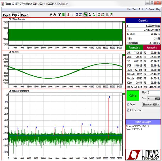
This circuit has an SNR of 82dBFS (Add full scale - F1 amplitude to SNR to get SNR in dBFS, in this case 82.091dBFS) and THD of –84dB as shown in the PScope plot of Figure 2. This is close to the typical specs for the LTC2323-16 indicating minimal performance degradation by the driver. Finding a signal generator capable of ±10V @ 2.2MHz with low THD was not possible so the input level shown is only –6dBFS. If higher input impedance is required the input can be buffered by an LT1363 op amp or equivalent. If differential inputs are required the circuitry around U1B can be duplicated for U1A instead of driving U1A from U1B.

Figure 2. PScope plot using the circuit of Figure 1


