Configuring the DS1831's Time Delays and Voltage Trip Levels in Multi-Power-Supply Systems
摘要
This application note describes how to set up the DS1831 for monitoring multi-voltage systems. It shows how to adjust delay time as well as adjusting trip thresholds. The application note also shows how the DS1831 can be used in systems with sequenced power supplies.
Introduction
DS1831's (see selection guide below) have several inputs that are used to configure the tolerance of the power supply monitoring and the length of delay associated with each power supply's reset. Additionally, the watchdog timer's strobe period can be adjusted using a similar input. To offer maximum design flexibility, each of the inputs can be placed into one of three states (grounded, connected to VCC, and disconnected), which allows three different configurations for the trip levels and timers. This is implemented by a circuit that samples each input shortly after the first of the two primary supplies becomes active. Once the settings are detected at power-up, they will remain set until the next time power is cycled. When the design requires one of the TOL or TD inputs to be connected to a supply voltage, the data sheet recommends connecting them to the corresponding power supply (e.g. TOL3.3V connected to IN3.3V). This is problematic when the two primary supplies do not come up at the same time because the TOL and TD inputs connected to the second power supply may appear to be grounded if that supply is off when the first supply is activated and the configuration inputs are sampled.
This application note explains how the DS1831 samples the configuration inputs and provides two circuit solutions to ensure the DS1831 is configured properly regardless of the order the power supplies are activated.
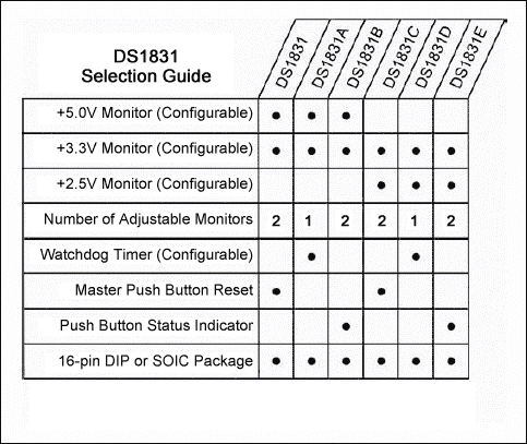
Figure 1. DS1831 feature selection guide.
Understanding the DS1831's Sampling Circuit
The "tricks" to configuring the DS1831 are understanding when it samples the TOL and TD inputs, and knowing that the TOL and TD inputs can be connected to voltages as high as 5.5V.
The DS1831 samples the TOL and TD inputs as the first of the two primary power supplies rises above the level that trips the DS1831's internal power on reset (POR). The reason the first supply to reach the POR level triggers the sampling is because the DS1831 powers itself from the higher of the two primary power supplies. Once the initial sample of the TOL and TD inputs is taken, the values determined by the sampling circuit are latched until the next time the part is powered up. Because the second power supply may still be at 0V when the configuration inputs are sampled, inputs connected to the second power supply may be detected as GND instead of VCC. The two sections below on using the DS1831 with sequenced and asynchronous power supplies provide workarounds to ensure the DS1831 can be configured correctly. Only DS1831 designs requiring at least one configuration input to be connected to VCC need to worry about this phenomenon. Designs requiring only GND and disconnect settings are not affected.
Although the data sheet recommends connecting the TOL and TD inputs to their corresponding power supply (e.g. TOL3.3V to IN3.3V), all of the TOL and TD inputs can handle voltages as high as 5.5V regardless of their corresponding power supply's level. This allows powering all of the configuration inputs requiring a VCC connection from the supply that powers up first, which can avoid having a configuration input connected to a non-activated VCC supply.
Using the DS1831 with Sequenced Power Supplies
In systems were the supplies come up in a predictable sequence (e.g. the 5.0V supply always rises before the 3.3V supply), all the TOL and TD inputs requiring VCC connections can be connected to the supply that comes up first. As mentioned before, all the TOL and TD inputs can handle connections to 5.5V without issue, so connecting the 3.3V TOL pin to the 5.0V supply does not cause an overvoltage issue.
Probably the most common power system configuration (see Figure 2) where the supplies are guaranteed to be sequential is when voltage regulators are used to generate subsequently lower and lower voltages. It is common for systems to have a 5.0V regulator that operates off a master power source, and a 3.3V regulator that operates from 5.0V regulator's supply. Because the 3.3V regulator is dependent on the 5.0V supply, it will always come up sometime after the 5.0V supply. In systems with similar timing to this example, the 5.0V supply can be connected to all the 5.0V and 3.3V configuration inputs that require VCC connections.
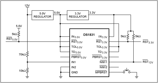
Figure 2. DS1831 sequenced power supply example circuit.
Using the DS1831 with Asynchronous Power Supplies
In systems where either power supply can come up first, external diodes can be used to ensure that the TOL and TD inputs that require VCC connections are at the correct level during sampling regardless of which supply is activated first. Figure 3 shows how connect the diodes to the DS1831. The 1MΩ resistor is required to provide a path for voltage on the VCC connected configuration pins to discharge when both supplies are powered-down. This prevents the otherwise high impedance node from retaining its high state voltage on power-down, which could damage an input by remaining at a high state without either VCC powered.
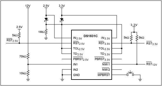
Figure 3. Ensuring TOL and TD are high when sampled on power-up.
Design Notes
Although decoupling capacitors are not shown on either circuit diagram, high-quality, surface-mount, ceramic decoupling capacitors (0.01µF to 0.1µF) should be located near each of the part's supplies to prevent VCC glitches from activating the reset circuitry. All the reset outputs including the NMI outputs are open drain outputs that require pull-up resistors to reach high levels. If the VCC diode circuit is required for a particular application, one set of diodes with the 1MΩ pull-down resistor can be used for all the TOL and TD inputs requiring VCC connections. There is no need to replicate the diode circuitry for each TOL or TD input.
Conclusions
The DS1831 samples its TOL and TD configuration pins during the power-up of the first of its two main power supplies. Designs utilizing the DS1831 that require one of the configuration pins to be connected to VCC must ensure that the configuration pin is high by the sampling time. If one supply always rises before the other, the configuration pins requiring a VCC connection can be connected to the first supply. If either supply can be brought up first, the design can utilize the diode circuit shown in Figure 3 to ensure that the TOL and TD configuration pins that require VCC connections are detected properly. If these precautions are not taken, the DS1831 may detect and latch the wrong configuration settings on power-up, which will require the system's power to be cycled to correct the problem.


