摘要
Electronic loads require protection from the effects of power outages and fluctuations, inductive load switching, and lightning. In this design solution, we review a typical protection solution with a low level of integration that creates inefficiencies in PC board space and a higher bill of materials. We will examine how a new family of integrated, highly flexible protection ICs with low RDS(ON) provides direct, reverse-voltage and current protection. With a smaller bill of materials and better utilization of PC board space, these new ICs build a perimeter of protection around the load for enhanced safety and reliability.
Introduction
Protection circuits are the unsung heroes of modern electronics. The long electric chain, from the AC line to the digital load, no matter the application, is interspersed with fuses and transient voltage suppressors of all sizes and shapes. Along the electrical path, electrical stressors—such as inrush currents due to storage capacitors, reverse currents due to power outages, overvoltages, and undervoltages induced by inductive load switching or lightning—can damage precious electronic loads. This is true for microprocessors and memories, which are built with fragile sub-micron, low-voltage technologies. Like the pioneers of the old west circling the wagons, it is necessary to build a perimeter of protection around the load to handle these potentially catastrophic events (Figure 1).
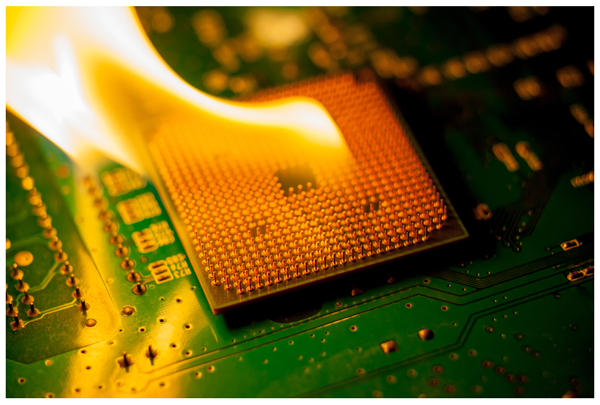 Figure 1. Unprotected CPU on fire.
This design solution first reviews the fundamental features of an effective protection scheme. Subsequently, it highlights the shortcomings of a typical protection implementation, such as high bill of materials and PC board size occupation. Finally, it introduces a new family of integrated, highly flexible protection ICs that address these concerns.
Typical System Protection
Figure 2 shows a typical system protection scheme around the smart load, for example, a microprocessor. A DC-DC converter—complete with control (IC2), synchronous rectification MOSFETs (T3, T4) and associated intrinsic diodes (D3, D4), and input and output filter capacitors (CIN, COUT)—powers the microprocessor. A voltage surge that comes from the 48V power bus (VBUS), if directly connected to VIN, would have catastrophic consequences for the DC-DC converter and its load. For this reason, front-end electronic protection is necessary. Here the protection is implemented with a controller (IC1) that drives two discrete MOSFETs T1 and T2.
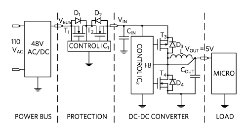 Figure 2. Typical electronic system and protection.
The protection electronics must handle fault conditions like overvoltage/undervoltage, overcurrent and reverse current flow within the limits of its voltage and current rating. If the expected voltage surge exceeds the protection electronics rating discussed here, additional layers of protection can be added, in the form of filters and transient voltage suppression (TVS) devices.
Overvoltage Protection
If the DC-DC converter's maximum operating voltage is 60V, the protector IC will consist essentially of a MOSFET switch (T2) that is closed within this operating range and open above it. The associated intrinsic diode D2 is reverse-biased in case of overvoltage and does not play a role. The presence of T1/D1 is also inconsequential in this case, with T1 fully "on."
Overcurrent Protection
Even when the incoming voltage is confined within the allowed operating range, problems can persist. Upward voltage fluctuations generate high CdV/dt inrush currents that can blow a fuse or overheat the system, reducing its reliability. Accordingly, the protection IC must be equipped with a current limiting mechanism.
Reverse-Current Protection
A MOSFET's intrinsic diode between drain and source is reverse-biased when the MOSFET is "on" and forward-biased when the MOSFET voltage polarity reverses. It follows that T2 by itself will not block negative-input voltages. These can happen accidentally, for example, during a negative transient or a power outage, when the input voltage (VBUS in Figure 2) is low or absent and the DC-DC converter input capacitor (CIN) feeds the power BUS via the intrinsic diode D2. To block the reverse current, the transistor T1, placed with its intrinsic diode D1 opposing the negative current flow, is necessary. The result is a costly back-to-back configuration of two MOSFETs with their intrinsic diodes oppositely biased.
Integrated Back-to-Back MOSFETs
The need for a back-to-back configuration is obvious if discrete MOSFETs are utilized, like in Figure 2, and less obvious if the protection is monolithic, namely when the control circuit and MOSFET are integrated in a single IC. Many integrated protection ICs equipped with reverse-current protection utilize a single MOSFET, with the additional precaution of switching the device body-diode to reverse-bias no matter the MOSFET polarization. This implementation works well with 5V MOSFETs, which have a symmetrical structure with respect to source and drain. Source-body and drain-body maximum operative voltage are here the same. High-voltage MOSFETs, in our case, are not symmetrical and only the drain is designed to withstand high voltage with respect to body. Layout of high-voltage MOSFETs is more critical and HV MOSFETs with optimized RDS(ON) come only with the source shorted to the body. Bottom line, a high-voltage (> 5V) integrated solution must utilize a back-to-back configuration as well.
Motor Drive Applications
In motor driver applications, the DC motor current is PWM-controlled with a MOSFET bridge driver. During the OFF-portion of the PWM control cycle, the current recirculates back to the input capacitor, effectively implementing an energy recovery scheme. In this case, reverse-current protection is not called for.
Traditional Discrete Solution
Figure 3 illustrates the high costs, in terms of PC board area and bill of materials, of utilizing a discrete implementation like the one in Figure 2 (24VIN, -100V to +40V protection). The PC board area is a hefty 70mm2.
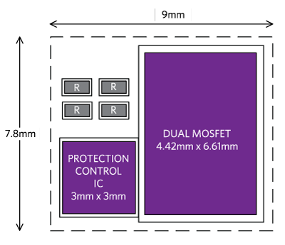 Figure 3. Traditional discrete protection (70mm2).
Integrated Solution
Figure 4 shows the advantage of integrating the control and power MOSFETs in the same IC, packaged in a 3mm × 3mm, TDFN-EP package. In this case, the PC board area occupation is down to roughly 40% of the discrete solution (28mm2).
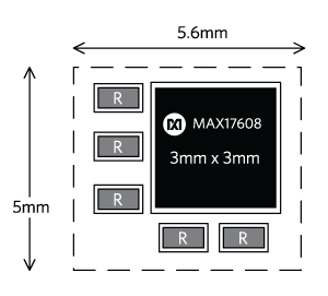 Figure 4. Integrated protection (28mm2)
Integrated Protection Family
The MAX17608/MAX17609/MAX17610 family of adjustable overvoltage and overcurrent protection devices provides an example of such an integrated solution. It features a low, 210mΩ, on-resistance integrated FET. The devices protect downstream circuitry from positive and negative input voltage faults up to ±60V. The overvoltage-lockout threshold (OVLO) is adjusted with optional external resistors to any voltage between 5.5V and 60V. Also, the undervoltage-lockout threshold (UVLO) is adjusted with optional external resistors to any voltage between 4.5V and 59V. They feature programmable current-limit protection up to 1A. The current-limit threshold can be programmed by connecting a suitable resistor to the SETI pin. The MAX17608 and MAX17610 block current flow in reverse direction, whereas the MAX17609 allows current to flow in reverse direction. The devices also feature thermal shutdown protection against internal overheat. They are available in a small, 12-pin (3mm × 3mm) TDFN-EP package. The devices operate over the -40°C to +125°C extended temperature range.
Conclusion
Electronic loads require protection from the effects of power outages and fluctuations, inductive load switching, and lightning. We reviewed a typical protection solution, with its low level of integration that leads to inefficiencies in terms of PC board space and high bill of materials. A new family of integrated, highly flexible, low RDS(ON) protection ICs provides direct and reverse voltage and current protection with a minimum bill of materials and PC board space occupation. With MAX17608, MAX17609, and MAX17610, "the wagons" are tightly circled, building a perimeter of protection around the load for enhanced safety and reliability.


